OLED display panel and preparation method thereof

A technology for display panels and glass substrates, applied in semiconductor/solid-state device manufacturing, electrical components, electrical solid-state devices, etc., can solve problems affecting display, corrosion of via hole structures, etc., to increase charging speed, reduce charging time, and improve display The effect of the characteristic

Active Publication Date: 2019-08-23
SHENZHEN CHINA STAR OPTOELECTRONICS SEMICON DISPLAY TECH CO LTD
View PDF4 Cites 10 Cited by
  • Summary
  • Abstract
  • Description
  • Claims
  • Application Information

AI Technical Summary

Problems solved by technology

[0004] The present invention provides a liquid crystal display panel, which can protect the through-hole structure corresponding to the frame glue from short circuit caused by water vapor corrosion, so as to solve the problem of existing liquid crystal display pan

Method used


Image

  • OLED display panel and preparation method thereof
  • OLED display panel and preparation method thereof
  • OLED display panel and preparation method thereof

Examples


Embodiment Construction

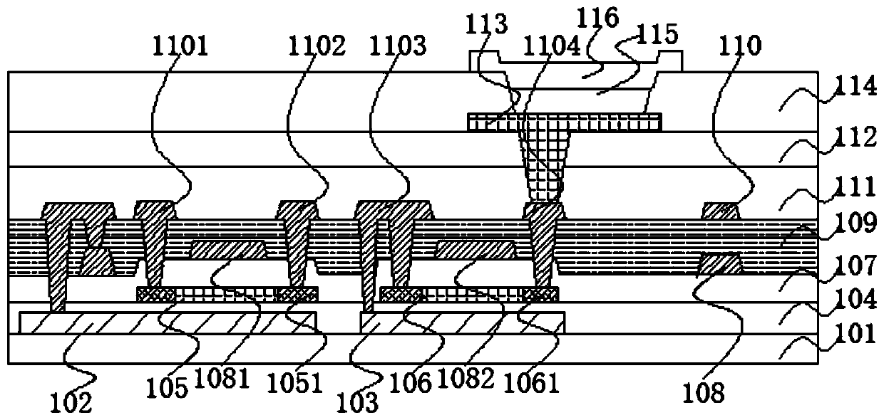
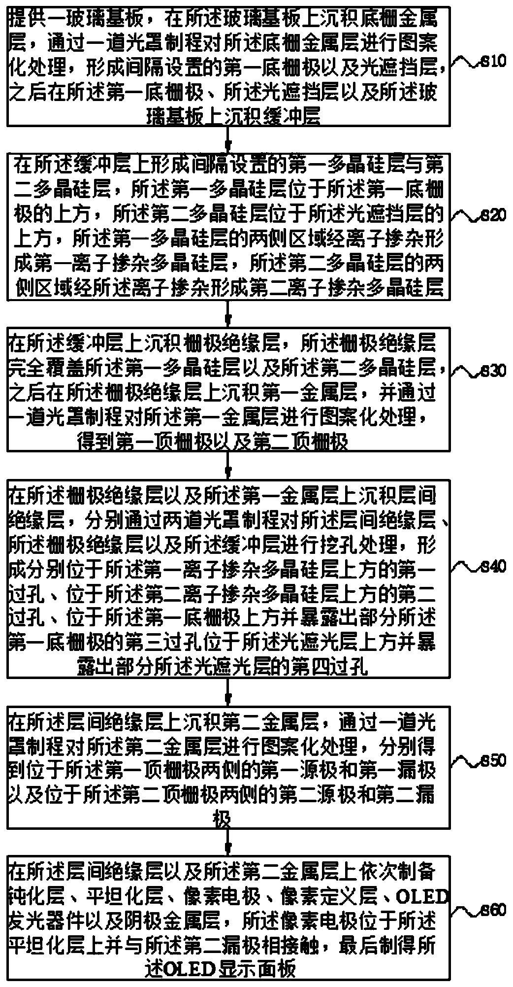
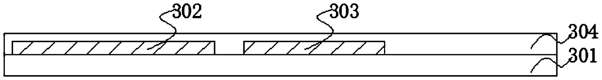
[0032] The following descriptions of the various embodiments refer to the accompanying drawings to illustrate specific embodiments in which the invention may be practiced. The directional terms mentioned in the present invention, such as [top], [bottom], [front], [back], [left], [right], [inside], [outside], [side], etc., are only for reference The orientation of the attached schema. Therefore, the directional terms used are used to illustrate and understand the present invention, but not to limit the present invention. In the figures, structurally similar elements are denoted by the same reference numerals.

[0033] The present invention is aimed at the existing OLED display panel and its preparation method. When the double-gate low-temperature polysilicon thin film transistor structure is used in the pixel drive circuit, it is difficult for the pixel drive circuit to reach the saturation current, resulting in a large pixel drive voltage, which further affects the OLED. Thi...


PUM


Abstract

The invention discloses an OLED display panel and a preparation method. The OLED display panel comprises a glass substrate, a first bottom gate, a light shielding layer, a buffer layer, a first polycrystalline silicon layer, a second polycrystalline silicon layer, a gate insulating layer, a first top gate, a second top gate, an interlayer insulating layer, a first source electrode, a first drain electrode, a second source electrode, a second drain electrode, a passivation layer, a planarization layer, a pixel electrode, a pixel definition layer, an OLED light-emitting device and a cathode metal layer. The first source electrode is in contact with the first bottom grid electrode through a via hole, and the second source electrode is in contact with the light shielding layer through anothervia hole.

Description

technical field [0001] The invention relates to the field of display technology, in particular to an OLED display panel and a preparation method thereof. Background technique [0002] With the development of the field of flat panel display, the panel display tends to be more and more high-frequency and high-resolution, and higher requirements are put forward for the panel driver. At present, the pixel driving circuit of AMOLED (active matrix light-emitting diode panel) display usually adopts TFT (thin film transistor) array substrate, and its carrier concentration is ten times that of amorphous silicon compared with amorphous silicon. TFT adopts low-temperature polysilicon (LTPS) material. Because of its high mobility, smaller TFTs can be used to drive the deflection of liquid crystal molecules, better meet the requirements of driving current, and are more and more widely used. It has been found in the prior art that double-gate low-temperature polysilicon thin-film transis...

Claims


Application Information

Patent Timeline
IPC IPC(8): H01L27/32H01L27/12H01L21/77
CPCH01L27/1251H01L27/1255H10K59/1213H10K59/1201
Inventor 姜云龙
Owner SHENZHEN CHINA STAR OPTOELECTRONICS SEMICON DISPLAY TECH CO LTD
Why Eureka
Try Eureka