Pixel defining layer, manufacturing method and display panel

A pixel definition layer and pixel definition technology, applied in semiconductor/solid-state device manufacturing, electrical components, electrical solid-state devices, etc., can solve problems such as long tailing of photoresist and affecting the size of pixel openings

Active Publication Date: 2019-08-23
BOE TECH GRP CO LTD
View PDF23 Cites 1 Cited by
  • Summary
  • Abstract
  • Description
  • Claims
  • Application Information

AI Technical Summary

Problems solved by technology

At present, in the process of using negative photoresist to prepare the pixel definition layer, due to the effect of optical scattering, the photoresist will have a long tail at the edge, which will affect the actual opening size of the pixel

Method used


Image

  • Pixel defining layer, manufacturing method and display panel
  • Pixel defining layer, manufacturing method and display panel
  • Pixel defining layer, manufacturing method and display panel

Examples


Embodiment Construction

[0036] In order to illustrate the present invention more clearly, the present invention will be further described below in conjunction with preferred embodiments and accompanying drawings. Similar parts in the figures are denoted by the same reference numerals. Those skilled in the art should understand that the content specifically described below is illustrative rather than restrictive, and should not limit the protection scope of the present invention.

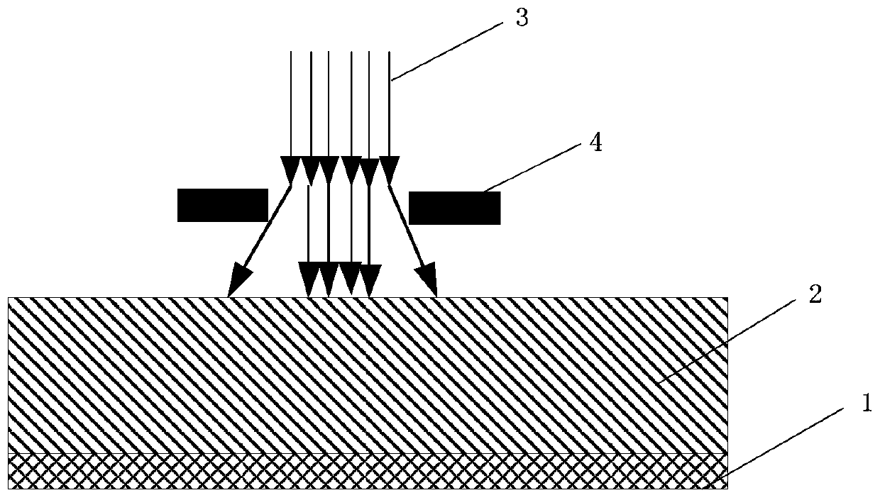
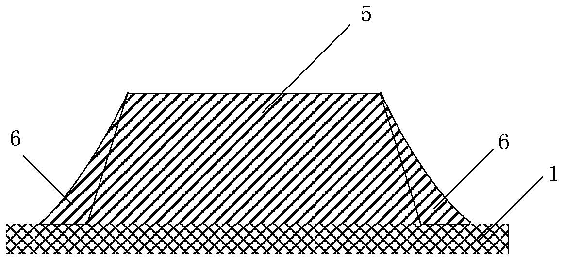
[0037] In the prior art, in the process of preparing the pixel defining layer using negative photoresist, such as Figure 1a As shown, a pixel-defining material layer 2 is formed on a substrate 1 , a mask 4 is arranged on the pixel-defining material layer 2 , and ultraviolet light 3 is irradiated to the pixel-defining material layer 2 from above the mask 4 . Such as Figure 1b Shown is the pixel defining layer 5 formed after exposure and development. The positive trapezoidal part in the figure is the pixel defining layer ...


PUM


Abstract

The invention discloses a pixel defining layer, a manufacturing method and a display panel. The pixel defining layer comprises a first pixel defining layer arranged on the substrate and a second pixeldefining area located at the side, away from the substrate, of the first pixel defining layer. The surface, close to the substrate, of the second pixel defining area and the surface, away from the substrate, of the first pixel defining layer have an annular non-overlapping area, and the orthographic projection, on the substrate, of the surface, close to the substrate, of the second pixel definingarea covers the orthographic projection, on the substrate, of the surface, away from the substrate, of the first pixel defining layer; the second pixel defining area comprises a second pixel defininglayer and an annular ultraviolet light absorption layer close to the first pixel defining layer, and the orthographic projection of the ultraviolet light absorption layer on the substrate covers theorthographic projection of the non-overlapping area on the substrate. According to the embodiment provided by the invention, through the arrangement of an ultraviolet light absorption layer, the trailing problem of the pixel defining layer caused by light scattering in the exposure process can be solved.

Description

technical field [0001] The invention relates to the field of display technology, in particular to a pixel defining layer, a manufacturing method and a display panel. Background technique [0002] Compared with LCD, Organic Light-Emitting Diode (OLED) has the advantages of self-luminescence, fast response, wide viewing angle, high brightness, bright color, light and thin, etc., and is considered to be the next generation display technology. [0003] The thin film deposition methods of organic material films for organic electroluminescent devices mainly include vacuum evaporation and solution process: 1. Vacuum evaporation is suitable for small organic molecules. Its film formation is uniform and the technology is relatively mature, but the investment in equipment is large. 1. Low material utilization rate and low alignment accuracy of large-sized products; 2. Solution process, including spin coating, inkjet printing, nozzle coating method, etc., is suitable for polymer materi...

Claims


Application Information

Patent Timeline
Patent Type & Authority Applications(China)
IPC IPC(8): H01L27/32H01L51/56
CPCH10K59/122H10K71/00H10K59/173H10K50/865H10K59/1201
Inventor 侯文军
Owner BOE TECH GRP CO LTD
Why Eureka
Try Eureka