Silicon-based Bi2O2Se structure terahertz wave switch

A terahertz, silicon-based technology, applied in the field of terahertz wave switching, can solve the problems of scarcity and backwardness of research data and results, and achieve the effects of superior performance, novel materials and simple structure

Active Publication Date: 2019-08-30
中国计量大学上虞高等研究院有限公司
View PDF6 Cites 2 Cited by
  • Summary
  • Abstract
  • Description
  • Claims
  • Application Information

AI Technical Summary

Problems solved by technology

However, limited by high-sensitivity detectors and efficient terahertz sources, research data and achievements in this frequency band have been relatively scarce for a long time, making the development of terahertz bands lag behind other bands.

Method used


Image

  • Silicon-based Bi2O2Se structure terahertz wave switch
  • Silicon-based Bi2O2Se structure terahertz wave switch
  • Silicon-based Bi2O2Se structure terahertz wave switch

Examples


Embodiment 1

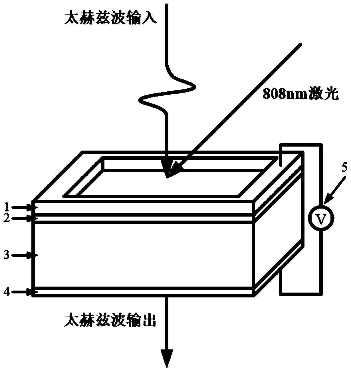
[0020] In this example, silicon-based Bi 2 o 2 The structure of the Se-structured terahertz wave switch and the shapes of the components are as described above, so details will not be repeated here. However, the specific parameters of each component are as follows:

[0021] The electrode material of the upper metal square ring is copper, the outer side is 1.5cm, the ring width is 0.5cm, and the thickness is 200nm. Bi 2 o 2 The Se nano film is square, with a side length of 1.5 cm and a thickness of 30 nm. The resistivity of the silicon substrate is greater than 10000Ωcm, the shape is square, the side length is 1.5cm, and the thickness is 500μm. The electrode material of the lower metal square ring is copper, the outer length is 1.5 cm, the ring width is 0.5 cm, and the thickness is 200 nm. The voltage source is a DC stabilized power supply, and the voltage adjustable range is 0V to 10V. The terahertz wave is vertically injected into the geometric center of the top layer ...


PUM

PropertyMeasurementUnit
thicknessaaaaaaaaaa
lengthaaaaaaaaaa
thicknessaaaaaaaaaa

Abstract

The invention discloses a silicon-based Bi2O2Se structure terahertz wave switch comprising an upper metal square ring electrode, a Bi2O2Se nano film, a silicon substrate, a lower metal square ring electrode and a voltage source, wherein the upper metal square ring electrode is located on the top layer, the lower layer of the upper metal square ring electrode is the Bi2O2Se nano film layer, the lower layer of the Bi2O2Se nano film layer is the silicon substrate, the lower layer of the silicon substrate is the lower metal square ring electrode, the upper metal square ring electrode and the lowermetal square ring electrode have the same size and shape and are connected by the voltage source, the terahertz wave is perpendicularly injected from the top layer into the top geometric center, thecontinuous laser of 808nm wavelength is injected from the top layer at 45 degrees into the top geometric center, and the switching control of the terahertz wave is realized by adjusting the continuouslaser power and the applied voltage. The silicon-based Bi2O2Se structure terahertz wave switch provided by the invention has the advantages such as novel material, simple structure, convenient manufacture and superior performance, and can be used for terahertz wave switch control.

Description

technical field [0001] The invention relates to a terahertz wave switch, in particular to a silicon-based Bi 2 o 2 Se structured terahertz wave switch. Background technique [0002] Terahertz generally refers to electromagnetic waves with a frequency of 0.1-10THz. Its frequency range is located in the intersection area of ​​electronics and photonics. Part of its low-frequency band overlaps with millimeter waves, and part of its high-frequency band overlaps with infrared bands. In the electromagnetic spectrum, terahertz waves are in a special frequency band position, and have many properties that millimeter waves and infrared bands do not have, which makes terahertz technology have very important research value in many aspects, and therefore has broad application prospects , has attracted the attention of governments and scientific research institutions around the world. However, limited by high-sensitivity detectors and efficient terahertz sources, research data and resul...

Claims


Application Information

Patent Timeline
Patent Type & Authority Applications(China)
IPC IPC(8): G02F1/01G02F1/00H01P1/10
CPCG02F1/0121G02F1/0126G02F1/0009H01P1/10G02F2203/13Y02P70/50
Inventor 李九生胡慕姝
Owner 中国计量大学上虞高等研究院有限公司
Why Eureka
Try Eureka