
Ion beam frequency modulation method based on surface acoustic waves

A surface acoustic wave and ion beam technology, applied in electrical components, impedance networks, etc., can solve problems such as large dispersion, poor controllability of chemical frequency modulation, and low product accuracy

Pending Publication Date: 2019-08-30
CHINA ELECTRONICS TECH GRP CORP CHONGQING ACOUSTIC OPTIC ELECTRONICS CO LTD
View PDF6 Cites 0 Cited by
  • Summary
  • Abstract
  • Description
  • Claims
  • Application Information

AI Technical Summary

Problems solved by technology

The controllability of chemical frequency modulation is not good, and the dispersion after adjustment is large, which is not suitable for scientific research and production. It has the disadvantages of poor product repeatability and consistency, and low product accuracy.

Method used


Image

  • Ion beam frequency modulation method based on surface acoustic waves
  • Ion beam frequency modulation method based on surface acoustic waves
  • Ion beam frequency modulation method based on surface acoustic waves

Examples


Embodiment 1

[0028] The purpose of this embodiment is to implement a series of processes for project 1 with high frequency accuracy (40ppm) of the sound meter project, etch project 1, frequency modulation target: require 2 pieces to reduce the target frequency 100-500Khz; 1 piece to increase the target frequency 100-500Khz .

[0029] Table 1 Comparison table before and after the implementation of item 1

[0030]

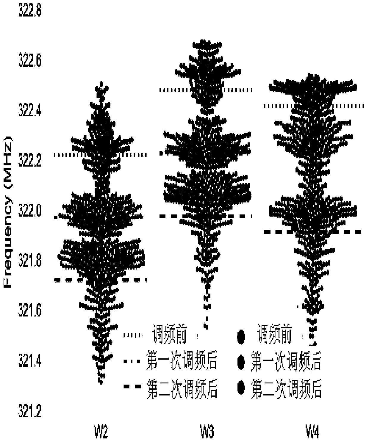
[0031] In this example, if figure 1 As shown, in order to further improve the dispersion of the device frequency and the target frequency, a second frequency modulation is performed to achieve the target frequency and reduce the frequency dispersion.

Embodiment 2

[0033] In this embodiment, a series of process implementation is carried out for item 2 with high frequency accuracy (40ppm), etching item 2, frequency modulation target: frequency control target 670.72±0.03Mhz, it is required to reduce the target frequency for 2 chips (chip 1#, 2#), 2 chips (chip 3#, 4#) can increase the target frequency, and the frequency consistency within the chip is improved.

[0034] Table 2 Comparison table before and after the implementation of project 2

[0035]

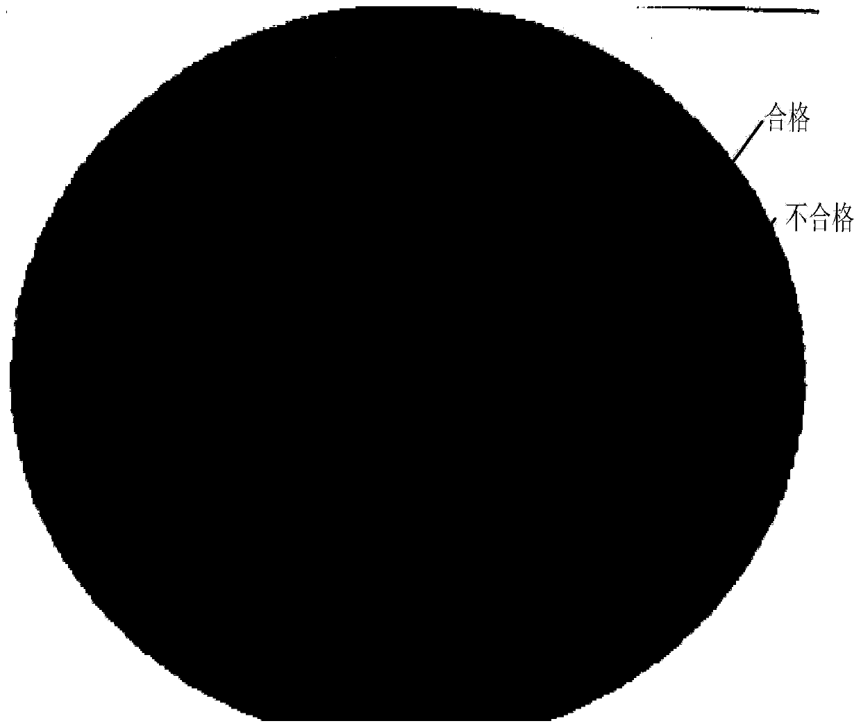
[0036] In this embodiment, the process implementation of the project with a frequency accuracy of 40ppm is verified. After frequency modulation, the target frequency is increased and decreased respectively, and the statistics figure 2 Qualification rate in , 1#, 2# wafers have a 25% pass rate before frequency modulation, and the pass rate distribution after frequency modulation is as follows image 3 ,statistics image 3 In the pass rate, the goal is achieved and the pass rate is incre...

Embodiment 3

[0038] In this embodiment, after the method of the present invention is implemented for the item 3 of the frequency accuracy 35ppm of the sound meter item, the test electrical performance analysis before and after the implementation is analyzed. In this example, Figure 4 It shows that the frequency is reduced from 275.58Mhz to 275.47Mhz after implementing the method, and the frequency of the wafer chip is increased from 275.35Mhz to 275.45Mhz after implementing the method.

[0039] The invention innovatively proposes for the first time that there is no SiO2 film on the surface in the professional production process of the acoustic meter, and the method of ion beam etching is used to increase or decrease the metal steps to achieve the purpose of reducing or increasing the frequency, and successfully solves the problem of line width and film In the production of high-frequency narrow-band surface acoustic wave devices with high thickness and high sensitivity, the use of the mos...


PUM


Abstract

The invention relates to the technical field of surface acoustic waves, in particular to an ion beam frequency modulation method based on surface acoustic waves, which comprises the following steps of: acquiring frequency distribution of a surface acoustic wave device by using a probe, and matching an actual wafer chip position and original frequency with equipment by using conversion software; obtaining the frequency, needing to be adjusted, of the chip, and calculating scanning parameters according to the substrate material, the surface oxide and different thicknesses of the chip to realizea target frequency value. In the frequency modulation process, argon ions are accelerated and bombarded on the surface of a wafer to remove redundant materials, and a frequency modulation layer film in the whole wafer range is scanned and etched, so that the filter frequency in the whole wafer range reaches a target value. According to the method, the frequency range can be increased or decreasedfrom 30khz to 20Mhz, and meanwhile, after part of projects use the technology, the test qualification rate is increased from 25% to 85%.

Description

technical field [0001] The present invention relates to the technical field of surface acoustic waves, in particular to an ion beam frequency modulation method based on surface acoustic waves (SAW). Background technique [0002] Surface acoustic wave devices are used in radar, communication and other weaponry electronic systems, and are the key components of the system. As the system puts forward higher precision and higher frequency requirements, higher requirements are also put forward for high-frequency narrow-band devices. The demand for high frequency accuracy of low-frequency narrow-band SAW devices and SAW high-frequency devices above 2Ghz is increasing. [0003] Under the current equipment capability, it is difficult to realize the production of this type of product, and only by adopting frequency modulation technology to improve the frequency accuracy. The commonly used frequency modulation techniques include physical frequency modulation and chemical frequency mod...

Claims


Application Information

Patent Timeline
IPC IPC(8): H03H3/10
CPCH03H3/10
Inventor 伍平陈峻赵雪梅米佳黎亮
Owner CHINA ELECTRONICS TECH GRP CORP CHONGQING ACOUSTIC OPTIC ELECTRONICS CO LTD
Learn More