Metal interconnecting structure and manufacturing method thereof

A technology of metal interconnection structure and manufacturing method, which is applied in semiconductor/solid-state device manufacturing, electrical components, electrical solid-state devices, etc., can solve the problems of short-circuit contact resistance, large grain size, uneven surface morphology, etc., and achieve enlarged openings Size, increase the contact area, reduce the effect of contact resistance

Inactive Publication Date: 2019-09-06
WUHAN XINXIN SEMICON MFG CO LTD
View PDF1 Cites 4 Cited by
  • Summary
  • Abstract
  • Description
  • Claims
  • Application Information

AI Technical Summary

Problems solved by technology

However, the new interconnect structure is not perfect, and there are inevitably various problems
For example, in the aluminum-copper interconnection process, due to the large grains of aluminum, uneven surface morphology, and poor thickness uniformity, when the aluminum is connected through copper, the contact between copper and aluminum is prone to short circuit or contact resistance. Abnormal conditions such as excessively large, thus affecting the performance and service life of the device

Method used


Image

  • Metal interconnecting structure and manufacturing method thereof
  • Metal interconnecting structure and manufacturing method thereof
  • Metal interconnecting structure and manufacturing method thereof

Examples


Embodiment Construction

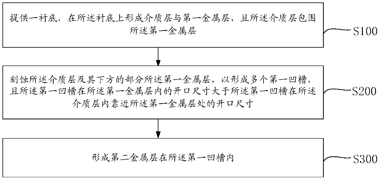
[0038] Based on the above problems, the present invention provides a method for fabricating a metal interconnection structure, comprising: providing a substrate, forming a dielectric layer and a first metal layer on the substrate, and the dielectric layer surrounds the first metal layer layer; etch the dielectric layer and part of the first metal layer below it to form a plurality of first grooves, and the opening size of the first grooves in the first metal layer is larger than the The size of the opening of the first groove in the dielectric layer close to the first metal layer; and forming a second metal layer in the first groove.

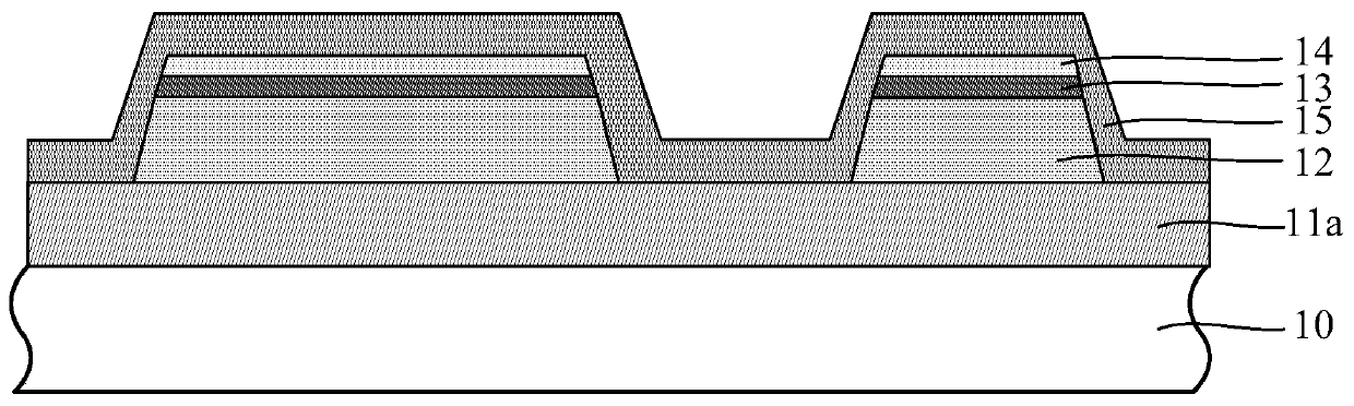
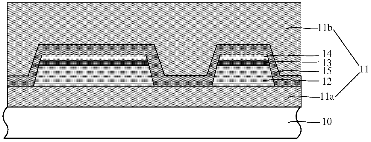
[0039] Correspondingly, the present invention also provides a metal interconnection structure, including: a substrate; a dielectric layer and a first metal layer located on the substrate, the dielectric layer surrounds the first metal layer, and the dielectric layer A plurality of first grooves are formed in the first metal layer and the part be...


PUM


Abstract

The invention provides a metal interconnecting structure and a manufacturing method thereof. The method comprises the following steps: providing a substrate, wherein a dielectric layer and a first metal layer are formed on the substrate, and the first metal layer is surrounded by the dielectric layer; etching the dielectric layer and a part of the first metal layer below the dielectric layer so asto form a plurality of first grooves, wherein the opening sizes, inside the first metal layer, of the first grooves are greater than those of the first grooves, at the positions close to the first metal layer, inside the dielectric layer; and forming a second metal layer inside the first grooves. The opening sizes of the first grooves inside the firs metal layer are enlarged, and the contact areaof the second metal layer and the first metal layer can be increased, so that the contact resistance between the first metal layer and the second metal layer is reduced, the contact performance of the first metal layer and the second metal layer is improved, and finally the performance of a semiconductor device is improved.

Description

technical field [0001] The invention relates to the technical field of semiconductor manufacturing, in particular to a metal interconnection structure and a manufacturing method thereof. Background technique [0002] The metal interconnection structure is an indispensable structure for semiconductor devices. In the semiconductor manufacturing process, the quality of the formed metal interconnect structure has a great influence on the performance of the semiconductor device. [0003] With the continuous advancement of VLSI process technology, the feature size of semiconductor devices has been continuously reduced, and the performance of semiconductor devices has become stronger and stronger. However, as the size of semiconductors continues to shrink, smaller and smaller interconnect structures carry higher and higher currents, and the response time requirements of interconnect structures are getting shorter and shorter. Traditional aluminum interconnect structures can no lon...

Claims


Application Information

Patent Timeline
Patent Type & Authority Applications(China)
IPC IPC(8): H01L21/768H01L23/538
CPCH01L21/76807H01L21/76816H01L23/5386
Inventor 叶国梁谢岩曾甜王嘉绮
Owner WUHAN XINXIN SEMICON MFG CO LTD
Why Eureka
Try Eureka