Evaporation mask, OLED display substrate, fabrication method of OLED display substrate and display device

A technology for display substrates and manufacturing methods, applied in the directions of vacuum evaporation plating, sputtering plating, ion implantation plating, etc., can solve the problems of increasing the production time and production cost of OLED display panels, and reduce production costs and reduce production costs. Time, the effect of improving productivity

Pending Publication Date: 2019-09-06
BOE TECH GRP CO LTD
View PDF5 Cites 6 Cited by
  • Summary
  • Abstract
  • Description
  • Claims
  • Application Information

AI Technical Summary

Problems solved by technology

However, this requires an additional manufacturing process to form a protective layer, that is, to additionally design

Method used


Image

  • Evaporation mask, OLED display substrate, fabrication method of OLED display substrate and display device
  • Evaporation mask, OLED display substrate, fabrication method of OLED display substrate and display device
  • Evaporation mask, OLED display substrate, fabrication method of OLED display substrate and display device

Examples


Example Embodiment

[0046] In order to make the technical problems, technical solutions and advantages to be solved by the embodiments of the present invention clearer, the following will describe in detail with reference to the drawings and specific embodiments.

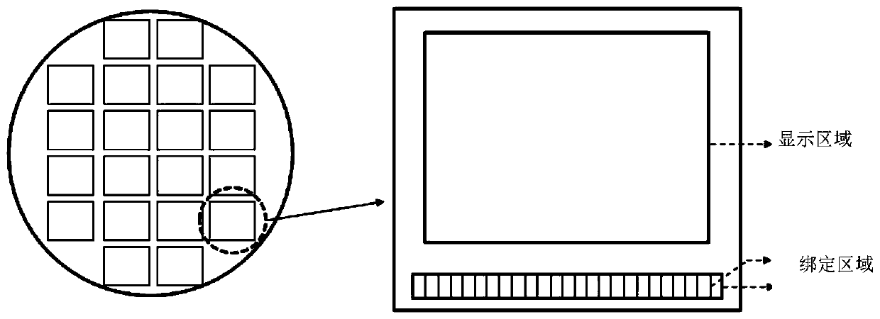
[0047] figure 1 It is a schematic diagram of the layout of the OLED display substrate on the silicon wafer, such as figure 1 As shown in the left half of , the silicon wafer is provided with multiple OLED display substrates arranged in an array; as figure 1 As shown in the right half of , a single OLED display substrate mainly includes a display area and a bonding area, wherein the bonding area is composed of a plurality of bonding pads, which are used as input signals of the OLED display substrate As with output channels, the bonding pads are made of metal.

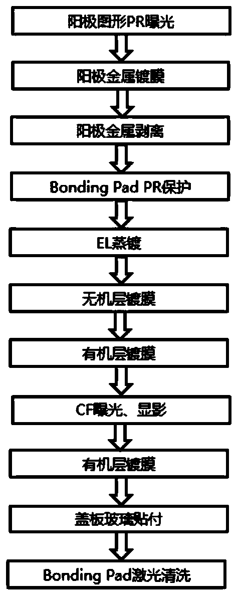
[0048] figure 2 It is a schematic diagram of the production process of the existing silicon-based OLED display panel, such as figure 2 As shown, the existing silicon-based ...


PUM


Abstract

The invention provides an evaporation mask, an OLED display substrate, a fabrication method of the OLED display substrate and a display device, and belongs to the technical field of display. The evaporation mask is used for fabricating an organic light-emitting layer of the OLED display substrate and comprises a first opening and a second opening, wherein the first opening is corresponding to a display region of the OLED display substrate, and the second opening is corresponding to a bonding region of the OLED display substrate. The fabrication method of the OLED display substrate comprises the steps of evaporating an organic light-emitting material on the substrate by the evaporation mask after a pattern of a positive electrode is fabricated on the substrate, and forming the organic light-emitting layer on the display region and the bonding region of the substrate. With the evaporation mask and the fabrication method of the OLED display substrate, provided by the technical scheme, theproduction time and the production cost of the OLED display substrate can be reduced.

Description

technical field [0001] The invention relates to the field of display technology, in particular to an evaporation mask, an OLED display substrate, a manufacturing method thereof, and a display device. Background technique [0002] At present, with the advancement of VR (virtual reality) / AR (augmented reality) technology and the rapid growth of the market, display panels suitable for VR / AR fields are also accelerating their pace towards miniaturization, high PPI (pixel density), The direction of rapid response and high color gamut is developing, and silicon-based micro-display OLED (organic electroluminescent diode) panels are just one of the prominent directions. Although silicon-based micro-display OLED started late, it is becoming a new focus of attention in the display field due to its advantages of miniaturization and high PPI. [0003] Currently, when making a silicon-based OLED display panel, a protective layer will be formed on the binding area of ​​the OLED display p...

Claims


Application Information

Patent Timeline
IPC IPC(8): H01L51/00H01L51/56C23C14/04C23C14/12C23C14/24
CPCC23C14/042C23C14/24C23C14/12H10K71/166H10K77/10H10K71/00Y02E10/549Y02P70/50
Inventor 卢鹏程黄冠达陈小川杨盛际董学王辉王晏酩
Owner BOE TECH GRP CO LTD
Why Eureka
Try Eureka