Display substrate, preparation method of display substrate and display panel

A display substrate and electrode technology, applied in semiconductor/solid-state device manufacturing, electrical components, electrical solid-state devices, etc., can solve the problems of weak light output in the edge area, decline in device luminous brightness and efficiency, and small effective light-emitting area, achieving reduction The effect of climbing volume, increasing the area of ​​effective light-emitting area, and alleviating the edge pinning effect

Active Publication Date: 2019-09-10
SUZHOU XINGSHUO NANOTECH CO LTD
View PDF4 Cites 8 Cited by
  • Summary
  • Abstract
  • Description
  • Claims
  • Application Information

AI Technical Summary

Problems solved by technology

In the prior art, the pixel defining layer is etched by the method of ordinary photomask, and the surface of the etched pixel defining layer is smooth, and after inkjet printing to the pixel area, it is easy to appear thin in the middle of the film surface, edge The thick climbing phenomenon makes the light output in the edge area weak, the effective light-emitting area is small, and the luminous brightness and efficiency of the device decrease

Method used


Image

  • Display substrate, preparation method of display substrate and display panel
  • Display substrate, preparation method of display substrate and display panel
  • Display substrate, preparation method of display substrate and display panel

Examples


Embodiment Construction

[0021] The technical solutions in the embodiments of the present application will be described in detail below in conjunction with the implementation manners of the present application. It should be noted that the described implementations are only some of the implementations of the present application, not all of the implementations.

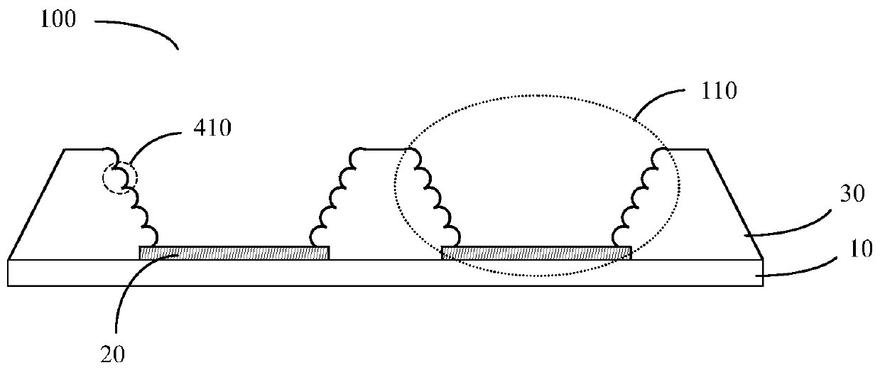
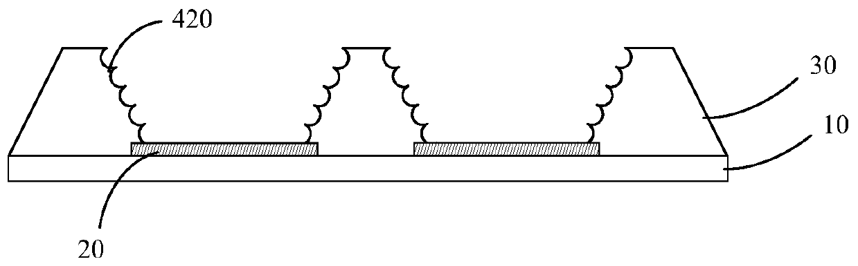
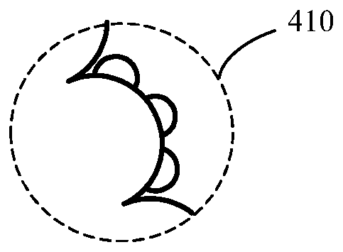
[0022] The embodiments of the present application are aimed at the preparation of quantum dot display devices by inkjet printing in the prior art. After the ink containing functional materials is printed to the designated pixel area, edge climbing occurs during the process of drying to form a film, and the display device emits light effectively. For the problems of small area and uneven luminous brightness, a display substrate and its manufacturing method and display panel are provided to solve the above problems, effectively alleviate the edge pinning effect caused by the evaporation of ink droplet solvent, and reduce the climbing volume of the...


PUM

PropertyMeasurementUnit
diameteraaaaaaaaaa
heightaaaaaaaaaa

Abstract

The invention provides a display substrate, a preparation method of the display substrate and a display panel. The display substrate comprises a substrate, a first electrode and a pixel defining layer, wherein the first electrode is arranged on the substrate; the pixel defining layer is arranged on the substrate and the first electrode; and the pixel defining layer defines a plurality of sub-pixelareas on the substrate, and the side wall of each sub-pixel area is provided with a microstructure surface. After ink-jet printing is carried out in the sub-pixel areas, ink drops can be prevented from climbing upwards along the edges by the microstructure surface in the process of drying and film forming of the ink drops, so that the uniformity of the film-forming thickness is ensured, and thenthe light-emitting uniformity of the display panel is further improved.

Description

technical field [0001] The present application belongs to the field of display technology, and in particular relates to a display substrate, a preparation method thereof, and a display panel. Background technique [0002] Colloidal quantum dots (QDs) are considered as alternative emissive materials for next-generation light-emitting diodes (LEDs) in lighting and display applications due to their high luminous efficiency, easily tunable emission wavelength, narrow half-peak width, and high color purity. Quantum dot light-emitting diodes (QLEDs) have attracted extensive attention in recent years due to their unique advantages such as wide color gamut, high color purity, high brightness, low turn-on voltage, and ultrathin size. [0003] For quantum dot light-emitting devices, inkjet printing technology has the advantages of simple operation and high material utilization, and can be applied in the preparation of large-area display devices. The preparation of QLEDs by inkjet pri...

Claims


Application Information

Patent Timeline
Patent Type & Authority Applications(China)
IPC IPC(8): H01L27/32H01L51/56
CPCH10K59/122H10K71/00
Inventor 王红琴史横舟王思元王允军
Owner SUZHOU XINGSHUO NANOTECH CO LTD
Why Eureka
Try Eureka