Schottky barrier diode

一种肖特基势、二极管的技术,应用在电气元件、电路、半导体器件等方向,能够解决正向电压增大、接触电阻增大等问题

Pending Publication Date: 2019-09-13
TAMURA KK
View PDF6 Cites 0 Cited by
  • Summary
  • Abstract
  • Description
  • Claims
  • Application Information

AI Technical Summary

Problems solved by technology

In addition, when the carrier concentration is lowered, the contact resistance with the ohmic electrode layer increases and the forward voltage (VF) increases.

Method used


Image

  • Schottky barrier diode
  • Schottky barrier diode
  • Schottky barrier diode

Examples


Embodiment 1

[0060] Next, more specific examples of the present invention will be described.

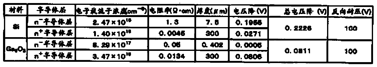
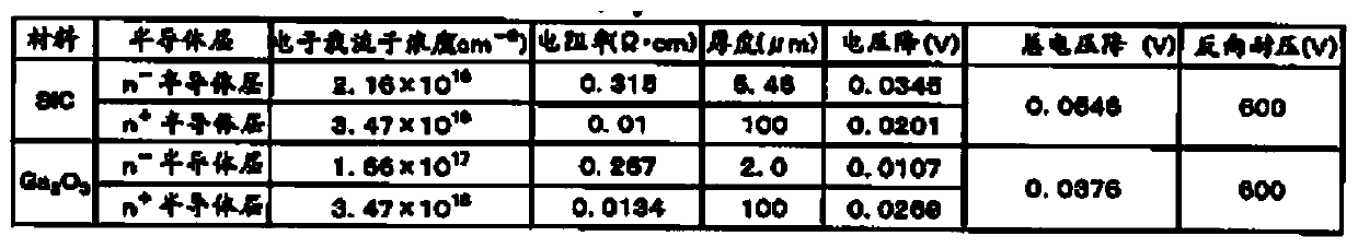
[0061] In this example, β-Ga 2 o 3 substrate as n + semiconductor layer 32 . In the β-Ga 2 o 3 substrate, doped with Si as a dopant, and formed with an electron carrier concentration of 1×10 19 cm -3 . In addition, the plane direction of the substrate was formed to be (010). Although the plane direction of the substrate is not particularly limited, it is preferably a plane rotated by an angle of 50° to 90° from the (100) plane. For example, there are (010) plane, (001) plane, (−201) plane, (101) plane, and (310) plane. In this way, re-evaporation from the substrate during epitaxial growth can be suppressed, and the growth rate can be increased. In addition, it may be a surface obtained by rotating the direction of the substrate surface by an angle of 37.5° or less from the (010) plane. In this case, it is possible to make n + Semiconductor layer 32 and n - The interface of the semico...

Deformed example 1

[0072] Figure 6A as well as Figure 6B A Schottky diode 1A showing a first modified example of the embodiment of the present invention, in which Figure 6A is a top view, Figure 6B yes Figure 6A A-A cutaway view.

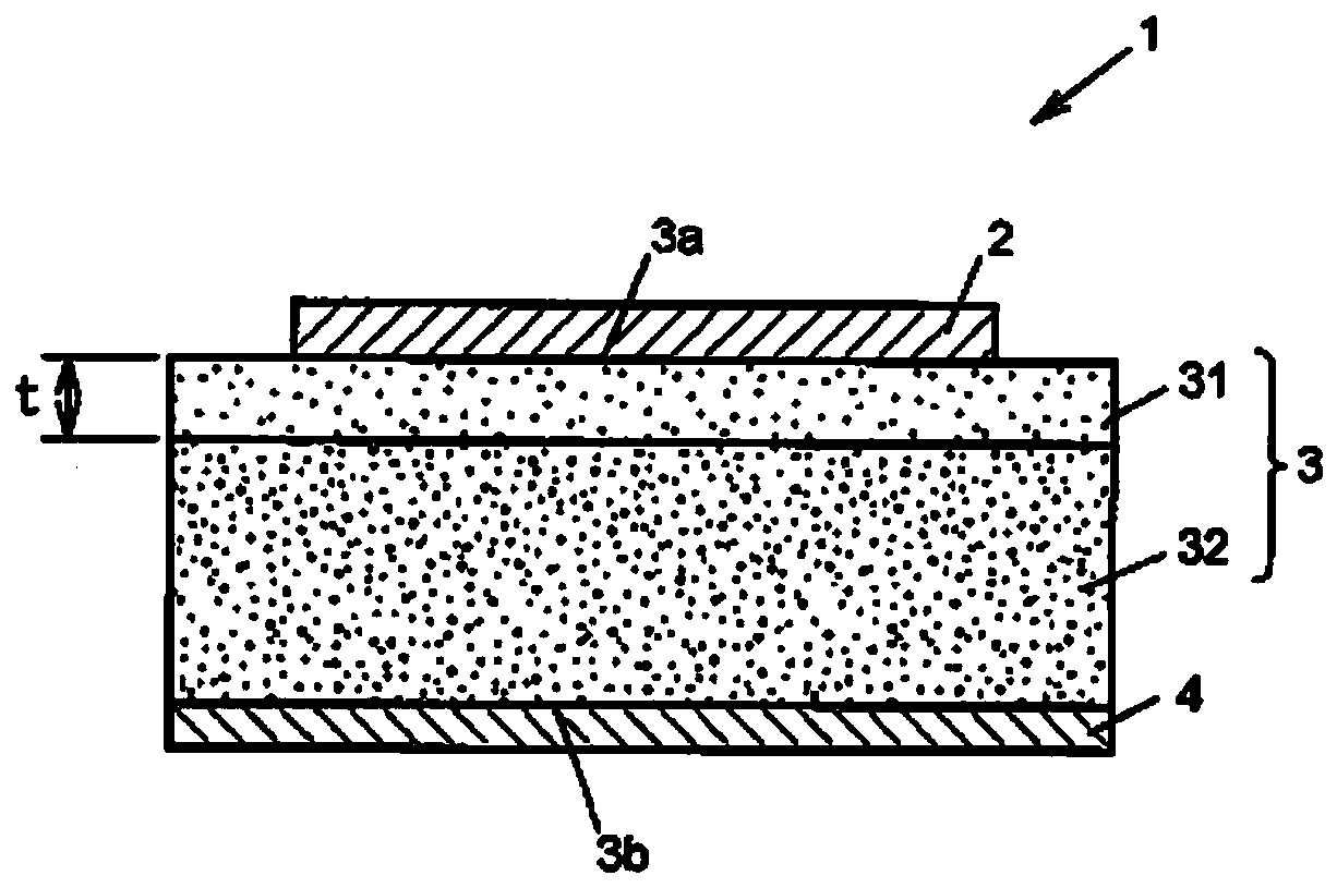
[0073] The Schottky diode 1A has a quadrangular shape in plan view, and a Schottky electrode layer 2 having a similar quadrangular shape is formed at the center thereof. In addition, the Schottky diode 1A includes an n-type semiconductor layer 3, and the n-type semiconductor layer 3 has an n-type semiconductor layer with a low electron carrier concentration. - The semiconductor layer 31, and having a ratio of the n - The n of the high electron carrier concentration of the high electron carrier concentration of the semiconductor layer 31 + semiconductor layer 32 . n for low electron carrier concentration - The semiconductor layer 31 is formed on the side of the n-type semiconductor layer 3 that is in Schottky contact with the Schottky electrode layer 2 . ...

Deformed example 2

[0078] Figure 7A as well as Figure 7B A Schottky diode 1B showing a second modified example of the embodiment of the present invention, in which Figure 7A is a top view, Figure 7B yes Figure 7A A-A cutaway view.

[0079] For Schottky diode 1B, at n - The structure in which the resistive layer 310 is formed on a part of the semiconductor layer 31 is different from the Schottky diode 1A, and the other structures are the same as the Schottky diode 1A. from n - The resistive layer 310 is formed on the upper surface 31 a side of the semiconductor layer 31 from the portion in contact with the peripheral portion of the Schottky electrode layer 2 to the side surface 31 b. The resistive layer 310 at n + Formed on the semiconductor layer 32 are n - Afterwards, the semiconductor layer 31 can be formed, for example, by annealing in an oxygen atmosphere. In addition, this region may be formed as a P-type layer instead of the resistance layer 310 .

[0080] According to the Sch...


PUM


Abstract

The invention provides a Schottky barrier diode capable of suppressing an increase in a forward voltage and an increase in a contact resistance with an ohmic electrode layer even when a reverse breakdown voltage is increased. A Schottky barrier diode (1) includes an n-type semiconductor layer (3) formed of a GaO-based compound semiconductor having n-type conductivity, and a Schottky electrode layer (2) coming into Schottky contact with the n-type semiconductor layer (3). The n-type semiconductor layer (3) has an n-semiconductor layer (31) which comes into Schottky contact with the Schottky electrode layer (2) and has comparatively low electron carrier concentration, and an n-semiconductor layer (32) having electron carrier concentration higher than that of the n-semiconductor layer (31) formed therein.

Description

[0001] This application is a divisional application, the application number of the original application is 201280054764.8, the international application number is PCT / JP2012 / 078983, the application date is November 08, 2012, and the invention name is "Schottky barrier diode". technical field [0002] The present invention relates to a Schottky barrier diode formed by contacting metal and semiconductor Schottky. Background technique [0003] Conventionally, a Schottky barrier diode using SiC is known as a high withstand voltage diode used, for example, in an inverter circuit (for example, refer to Patent Document 1). Schottky barrier diodes generally have a lower forward voltage (VF) and a shorter reverse recovery time (trr) than PN junction diodes with the same current capacity, and have excellent switching characteristics. However, people are eagerly pursuing higher withstand voltage and higher efficiency, and therefore seek further higher withstand voltage and lower forwar...

Claims


Application Information

Patent Timeline
Patent Type & Authority Applications(China)
IPC IPC(8): H01L29/872H01L29/06H01L29/24H01L21/02H01L21/34H01L29/47
CPCH01L21/02414H01L21/02433H01L21/02565H01L21/02576H01L21/02631H01L29/0619H01L29/0661H01L29/24H01L29/47H01L29/66969H01L29/872H01L29/045H01L29/267
Inventor 泷沢胜仓又朗人
Owner TAMURA KK
Why Eureka
Try Eureka