An insulated gate bipolar transistor and a manufacturing method thereof

A bipolar transistor and insulated gate technology, which is applied in the manufacture of semiconductor/solid-state devices, semiconductor devices, electrical components, etc., can solve the problem that the breakdown voltage of the device cannot be guaranteed at the same time. issues of sex

Inactive Publication Date: 2019-01-18
INST OF MICROELECTRONICS CHINESE ACAD OF SCI
View PDF5 Cites 0 Cited by
  • Summary
  • Abstract
  • Description
  • Claims
  • Application Information

AI Technical Summary

Problems solved by technology

[0004] Aiming at the problems existing in the prior art, an embodiment of the present invention provides an insulated gate double transistor and a manufacturing method thereof, which are used to solve the problem that the insulated gate d...

Method used


Image

  • An insulated gate bipolar transistor and a manufacturing method thereof
  • An insulated gate bipolar transistor and a manufacturing method thereof

Examples


Embodiment 1

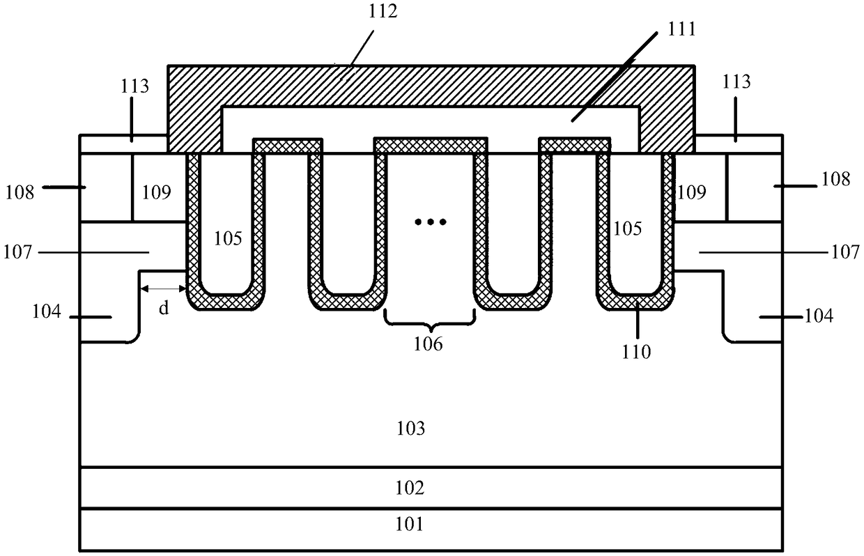
[0046] This embodiment provides an insulated gate bipolar transistor, such as figure 1 As shown, the insulated gate bipolar transistor includes: a substrate 101; a buffer layer 102, an epitaxial layer 103, a buried base region Base region 104, a trench gate 105, and a dummy region 106; wherein,

[0047] The substrate 101 is a SiC substrate of the first heavily doped type. The first heavily doped type may be N-type or P-type. The substrate 101 in this embodiment may be an N-type SiC substrate or a P-type. SiC substrate with a doping concentration of 10 18 ~10 19 cm -3 .

[0048] The buffer layer 102 is a second doping type SiC buffer layer, which is epitaxially formed on the substrate 101; the second doping type can be P-type or N-type, and the buffer layer 102 in this embodiment is a P-type SiC buffer Floor. The doping level and thickness of the buffer layer 102 can be specifically set according to the breakdown voltage, forward conduction voltage drop and dynamic characteristics ...

Embodiment 2

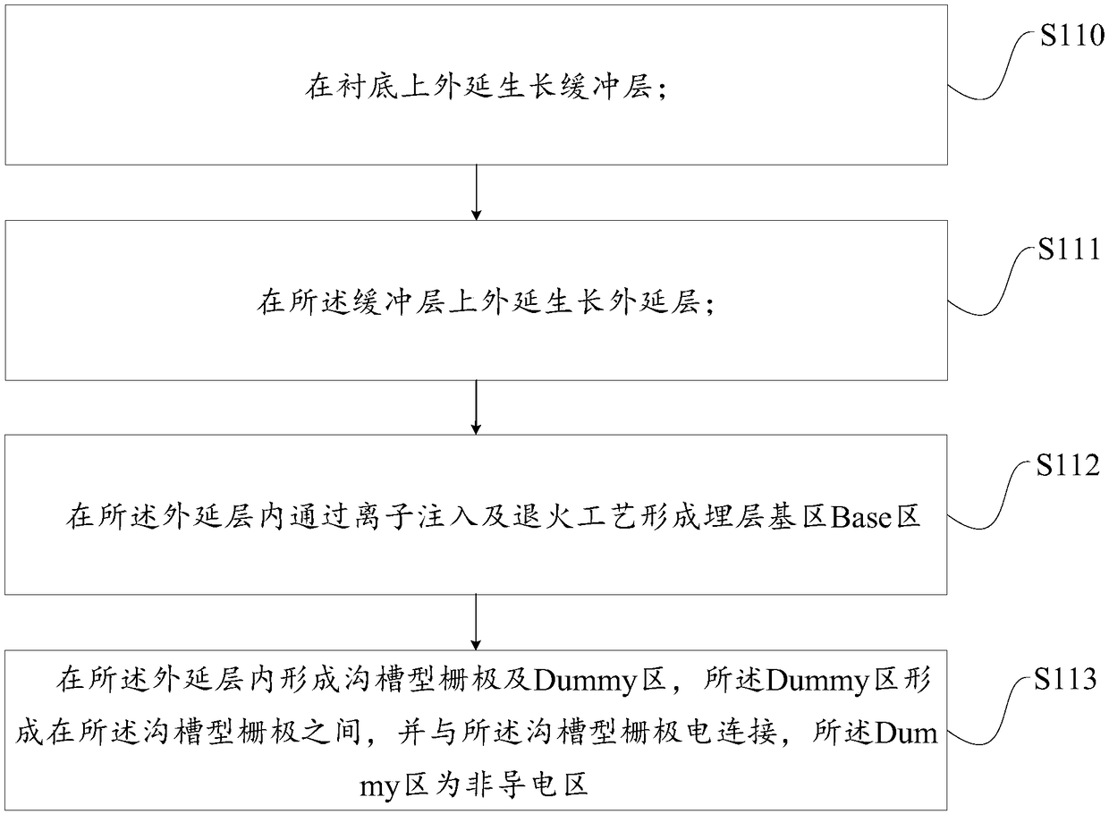
[0065] This embodiment provides a method for manufacturing an insulated gate bipolar transistor, such as figure 2 As shown, the method includes:

[0066] S110, epitaxially grow a buffer layer on the substrate;

[0067] The substrate in this embodiment is a first heavily doped SiC substrate, the first heavily doped type may be N-type or P-type, and the substrate in this embodiment may be an N-type SiC substrate or P-type SiC substrate with a doping concentration of 10 18 ~10 19 cm -3 .

[0068] The buffer layer is a SiC buffer layer of the second doping type, which is epitaxially formed on the substrate; the second doping type may be P-type or N-type, and the buffer layer in this embodiment is a P-type SiC buffer layer. The doping level and thickness of the buffer layer can be specifically set according to the breakdown voltage, forward voltage drop and dynamic characteristics of the transistor device. Dynamic characteristics refer to transistor switching characteristics and capac...


PUM

PropertyMeasurementUnit
Doping concentrationaaaaaaaaaa
Thicknessaaaaaaaaaa
Thicknessaaaaaaaaaa

Abstract

The invention provides an insulated gate bipolar transistor and a manufacturing method thereof. A buffer layer is formed on the substrate; An epitaxial layer is formed on the buffer layer. The buriedlayer base region is formed in the epitaxial layer. A trench gate is formed in the epitaxial layer; A Dummy region is for between that trench-type gates and electrically connected with the trench-typegates, and the Dummy region is a non-conductive region; The buried layer base region is located at one side of the trench gate, the buried layer base region is located below the source region, and the depth of the buried layer base region is larger than the depth of the trench gate in the longitudinal distribution; As such, that electric field strength at the bottom corn of the trench gate can bereduced, and the reliability and stability of the gate dielectric lay can be improved; As that trench gate make the transistor have a longitudinal channel, the resistance of the JFET region can be eliminated and the positive conduction voltage can be reduce; The Dummy region can increase the breakdown voltage, increase the cell pitch and optimize the channel orientation of the transistor, and further reduce the positive conduction voltage.

Description

Technical field [0001] The invention relates to the technical field of semiconductor devices, in particular to an insulated gate bipolar transistor and a manufacturing method thereof. Background technique [0002] The third-generation semiconductor material silicon carbide (SiC) has the advantages of large band gap, high critical breakdown field strength, high thermal conductivity and high electron saturation rate, and is very suitable for making high-voltage, high-temperature, high-frequency, and high-power semiconductor devices. [0003] In the design and preparation of silicon carbide insulated gate bipolar transistors, there are many challenges. The withstand voltage and reliability of the gate dielectric layer, the breakdown voltage of the device, the forward conduction voltage drop, and the dynamic characteristics all require attention. In the prior art, it is impossible to ensure the breakdown voltage of the device while reducing the forward voltage drop of the device and im...

Claims


Application Information

Patent Timeline
IPC IPC(8): H01L29/739H01L29/06H01L21/3105H01L21/336
CPCH01L21/3105H01L29/0649H01L29/66348H01L29/7397
Inventor 田晓丽谭犇宋瓘白云杨成樾刘新宇
Owner INST OF MICROELECTRONICS CHINESE ACAD OF SCI
Why Eureka
Try Eureka