Three-dimensional integrated structure for Micro LEDs and manufacturing method

A technology of three-dimensional integration and passivation layer, which is applied in the direction of electrical components, electrical solid devices, circuits, etc., can solve the problems of large area of ​​metal rewiring layer, complex structure of metal rewiring layer, large area of ​​MicroLED array, etc., and achieve reduction The effect of reducing the area, reducing the occupied area, and reducing the area

Pending Publication Date: 2019-09-13
XIAMEN SKY SEMICON TECH CO LTD
View PDF0 Cites 9 Cited by
  • Summary
  • Abstract
  • Description
  • Claims
  • Application Information

AI Technical Summary

Problems solved by technology

[0004] When the existing Micro LED array is connected to the driver chip, each Micro LED needs to be electrically connected to the pads of the driver chip, resulting in a large area of ​​the

Method used


Image

  • Three-dimensional integrated structure for Micro LEDs and manufacturing method
  • Three-dimensional integrated structure for Micro LEDs and manufacturing method
  • Three-dimensional integrated structure for Micro LEDs and manufacturing method

Examples


Embodiment 1

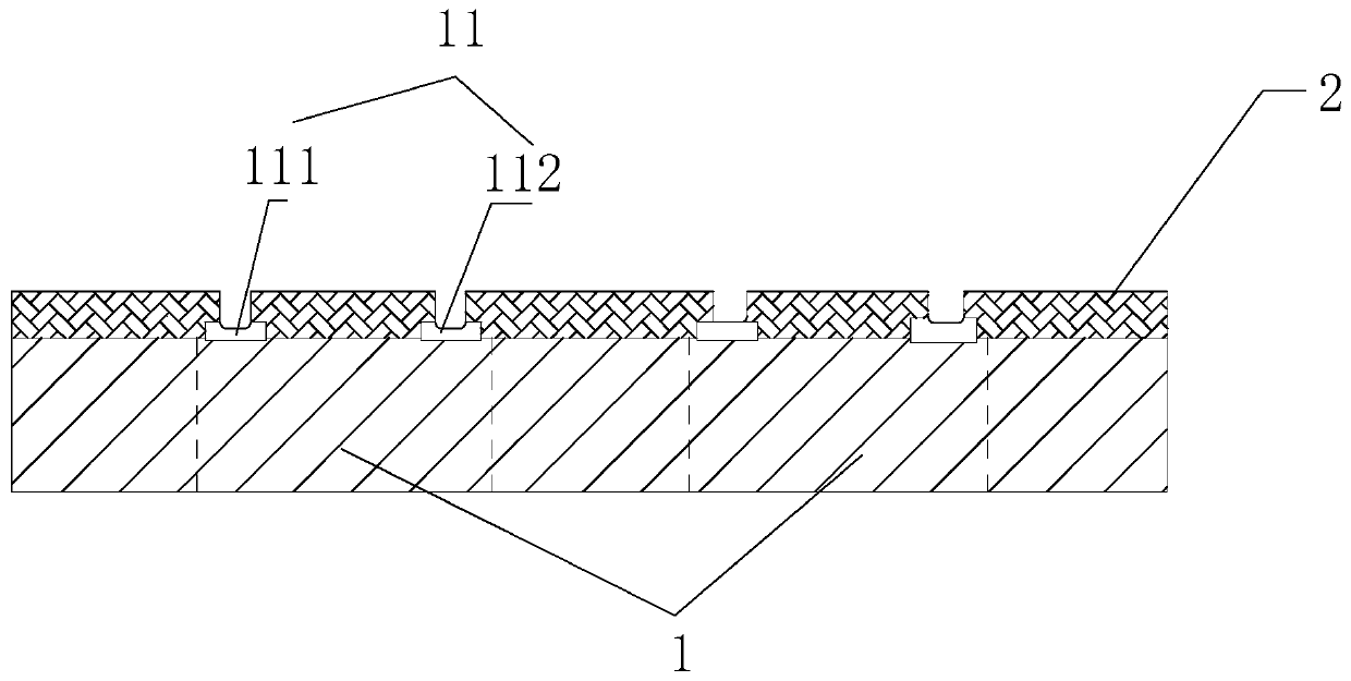
[0035] refer to Figure 1-Figure 4 , this embodiment provides a three-dimensional packaging method for Micro LEDs, including the following steps:

[0036] 1) Covering a layer of photoresist 2 on the Micro LED array 1 as the first insulating passivation layer;

[0037] 2) performing a photolithographic development process on the photoresist 2, opening holes in the photoresist 2 corresponding to the Micro LED pads 11, and exposing each of the Micro LED pads 11;

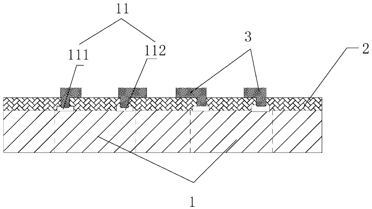
[0038] 3) Making the first metal wiring layer 3, the first metal wiring layer 3 is connected to the anode pad 111 of each of the Micro LEDs, and is also connected to the negative pad 112 of each of the Micro LEDs, and along the opening extending to the upper surface of the photoresist 2;

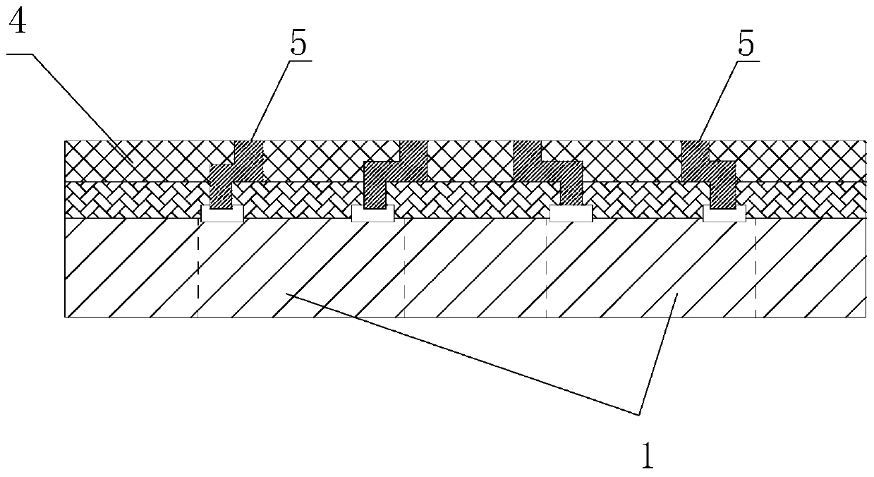
[0039] 4) Make a second insulating passivation layer 4 on the upper surface of the photoresist 2, cover the part of the first metal wiring layer 3 exposed on the upper surface of the photoresist 2, and expose the first metal wiring l...

Embodiment 2

[0054] refer to Image 6 The difference between this embodiment and Embodiment 1 is that: the first metal wiring layer 3 is divided into a first part 31 connected to the positive electrode pad 111 and a second part 32 connected to the negative electrode pad 112; the first part 31 and the second part The two parts 32 are detachable and located on the upper and lower horizontal planes. Since the first part 31 and the second part 32 have a height difference, the first part 31 and the second part 32 can overlap each other in the vertical direction to reuse the space and further reduce the area of ​​the first metal wiring layer 3 .

[0055] In order to avoid the mutual influence between the first part 31 and the second part 32, in this embodiment, the upper surface of the second insulating passivation layer 4 is also provided with a third insulating passivation layer 7, and the first part 31 is located on the first insulating passivation layer 4. layer and the second insulating pa...


PUM


Abstract

The invention provides a three-dimensional integrated structure for Micro LEDs. The three-dimensional integrated structure comprises a Micro LED chip array, a first insulation passivation layer, a first metal wiring layer, a second insulation passivation layer and at least one driver chip, wherein the first surface of the Micro LED array is covered with the first insulation passivation layer, andholes are formed in the first insulation passivation layer so as to expose positive bonding pads and negative bonding pads of the Micro LEDs; the first metal wiring layer is arranged on the upper surface of an insulating layer, and is connected with the positive bonding pads or the negative bonding pads of the chips; the second insulation passivation layer is arranged on the upper surface of the first metal wiring layer and the upper surface of the first insulation passivation layer, partial coverage of the upper surface of the first metal wiring layer is realized, and an exposed area is takenas an external connector; the at least one driver chip is provided with two or more than two bonding pads which are interconnected with metal electrodes on the first metal wiring layer respectively;and the driver chips are positioned on the upper surface of the second insulation passivation layer. The packaging area is reduced obviously, and simultaneously the thickness of the integral Micro Ledintegrated module is reduced.

Description

technical field [0001] The present invention relates to a structure and a manufacturing method of a Micro LED module, in particular to a structure and a manufacturing method of a Micro LED and a driver chip. Background technique [0002] Micro LED technology, that is, LED miniaturization and matrix technology; refers to the high-density micro-sized LED size integrated on a chip, such as each pixel of the LED display can be addressed and individually driven to light up, and the pixel level can be divided into millimeters down to the micron level. Micro LED not only inherits the advantages of high efficiency, high brightness, high reliability and fast response time of traditional LED, but also has the characteristics of energy saving, simple mechanism, small size, thin shape and no need for backlight. [0003] A typical structure of Micro LED is to have a PN junction diode, and the PN junction diode is composed of a direct energy gap semiconductor. At this stage, there are t...

Claims


Application Information

Patent Timeline
IPC IPC(8): H01L33/62H01L25/16H01L27/15
CPCH01L33/62H01L25/167H01L27/156H01L2933/0066
Inventor 于大全姜峰王阳红
Owner XIAMEN SKY SEMICON TECH CO LTD
Why Eureka
Try Eureka