

Semiconductor device and forming method thereof
A semiconductor and device technology, applied in the field of semiconductor devices and their formation, can solve the problems of poor performance of semiconductor devices, insufficient exposure and color saturation, reduce dark current, reduce the generation of photogenerated carriers, and improve picture quality. Effect
- Summary
- Abstract
- Description
- Claims
- Application Information
AI Technical Summary
Problems solved by technology
Method used
Image

Examples
Embodiment Construction
[0029] As described in the background, prior art semiconductor devices have poor performance.
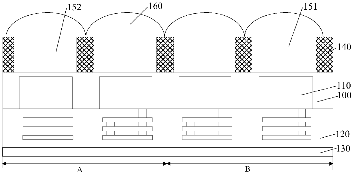
[0030] refer to figure 1 , figure 1 It is a structural schematic diagram of a semiconductor device, the semiconductor device includes: a plurality of color pixel units A and a plurality of black and white pixel units B located on the surface of a substrate 100, and the color pixel units A and black and white pixel units B include: interconnection layer 120, a photosensitive layer 110 and a light-receiving structure, the substrate 100 has an opposite first surface and a second surface; The light-receiving structure is located on the second surface of the substrate 100, the light-receiving structure includes a lens layer 160, a filter layer and a grid layer 140, the lens layer 160 is located on the surface of the filter layer, and the grid layer 140 is located on the adjacent surface. between the filter layers; the image sensor further includes a carrier plate 130 located on the sur...
PUM
 Abstract
Description
Claims
Application Information