Micro light emitting diode and display panel

A technology for light-emitting diodes and display panels, which is applied to electrical components, electrical solid-state devices, circuits, etc., and can solve problems such as difficulty, color shift, color spot, and misplacement

Active Publication Date: 2019-09-20
SHENZHEN CHINA STAR OPTOELECTRONICS SEMICON DISPLAY TECH CO LTD
View PDF2 Cites 4 Cited by
  • Summary
  • Abstract
  • Description
  • Claims
  • Application Information

AI Technical Summary

Problems solved by technology

However, because organic light emitting diodes are small in size and densely arranged, it is more difficult to apply the traditional manufacturing process to micro light emitting diodes to make display devices by single-sided printing, and the process of pasting and transposition is limited by the accuracy of the mechanism 1. The material properties of the stamp and the accuracy of the unit pitch (pitch) limit the resolution of the product, and when one side is pasted in a high-density arrangement, it is easy to generate interference from adjacent micro-LEDs during placement transposed, thus causing misplacing
[0006] In the active matrix drive display device (Active matrix, AM microLED), since the size of the micro-light-emitting diode display is usually smaller than 100um; its size exceeds the size of the traditional grabbing head, and the traditional binning cannot be used (bin) The machine divides the brightness, chromaticity, wavelength and voltage of the micro-light-emitting diode display chip into bins (bin), resulting in the micro-light-emitting diode display applied on the same display panel due to voltage, brightness, wavelength, and chromaticity. There are great differences, resulting in quality problems such as light and dark, color cast, and color spots

Method used


Image

  • Micro light emitting diode and display panel
  • Micro light emitting diode and display panel
  • Micro light emitting diode and display panel

Examples


Embodiment Construction

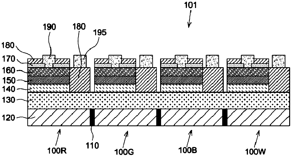
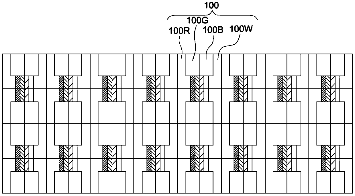
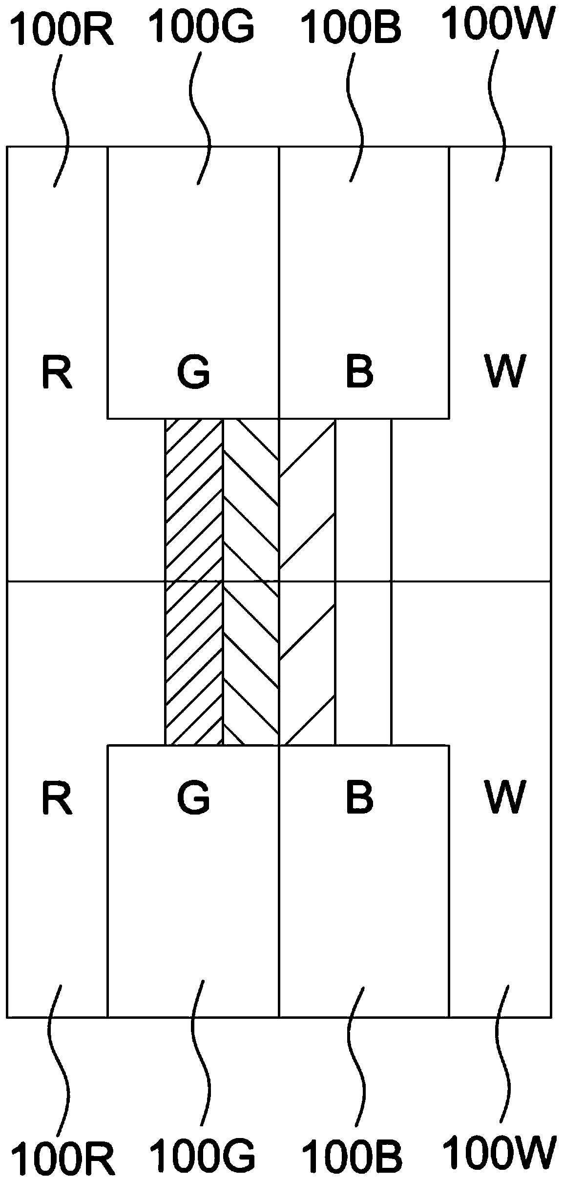
[0026] Please refer to the drawings in the accompanying drawings, wherein like reference numerals refer to like components. The following description is based on illustrated specific embodiments of the present application, which should not be construed as limiting other specific embodiments of the present application that are not described in detail here.

[0027] The following descriptions of the various embodiments refer to the accompanying drawings to illustrate specific embodiments in which the invention may be practiced. The directional terms mentioned in the patent of the present invention, such as "up", "down", "front", "back", "left", "right", "inside", "outside", "side", etc., are only Refer to attached drawings for directions. Therefore, the directional terms used are for explaining and understanding the present invention, but not for limiting the present invention.

[0028] In the drawings, the thickness of layers, films, panels, regions, etc., are exaggerated for...


PUM


Abstract

The invention provides a micro light emitting diode (101) and a display panel (300). The micro light emitting diode (101) comprises a light conversion layer (120) used for converting blue light into white light, a black matrix (110) arranged in the light conversion layer (120), a buffer layer (130) arranged on the light conversion layer (120), a first semiconductor layer (140) arranged on the buffer layer (130), an indium gallium nitride layer (150) arranged on the first semiconductor layer (140), a second semiconductor layer (160) arranged on the indium gallium nitride layer (150), a current spreading layer (170) arranged on the second semiconductor layer (160) and used for widening the light-emitting area, a passivation layer (180) arranged on the current spreading layer (170) and the buffer layer (130), a first cushion (190) and a second cushion (195).

Description

technical field [0001] The present application relates to the display field, in particular to a micro light emitting diode and a display panel. Background technique [0002] Nowadays, in order to pursue self-illumination to increase contrast and develop towards flexible displays, liquid-crystal displays (abbreviation: LCD) are developing towards organic electroluminescence displays (Organic Electroluminescence Display, abbreviation: OELD), OLED The advantage is that it can self-illuminate to meet the display requirements, does not require liquid crystals, and can make flexible and flexible displays, which is quite popular in the current stage of development. However, the disadvantages of OLED displays are that the manufacturing process is difficult, and the evaporation process and packaging process have not yet been optimized, followed by low process yield and increased production costs. [0003] At present, the industry uses Micro Light Emitting Diode Display (Micro LED fo...

Claims


Application Information

Patent Timeline
Patent Type & Authority Applications(China)
IPC IPC(8): H01L33/50H01L27/15
CPCH01L27/156H01L33/504
Inventor 樊勇
Owner SHENZHEN CHINA STAR OPTOELECTRONICS SEMICON DISPLAY TECH CO LTD
Why Eureka
Try Eureka