VCSEL device with high-dielectric-constant limiting hole and preparation method thereof

A high dielectric constant, current limiting technology, applied in electrical components, laser parts, circuits, etc., can solve the problems of inability to concentrate current in the middle of the device, affecting the heat dissipation and performance of the device, and excessive growth process requirements. The effect of strong repeatability, low production cost and reduced process time

Pending Publication Date: 2019-09-24
HEBEI UNIV OF TECH
View PDF6 Cites 3 Cited by
  • Summary
  • Abstract
  • Description
  • Claims
  • Application Information

AI Technical Summary

Problems solved by technology

Although the above-mentioned buried layer tunneling junction structure improves the lateral confinement of the current to a certain extent and improves the device performance to a certain extent, their device structures are relatively complicated, and the requirements for the growth process are too high, and the general industrial production level is more difficult to meet the standards proposed by the two devices
And using Al 2 o 3 When the hole is used as a current confinement hole, although the heat dissipation of the device is improved, it only uses the non-conductivity of the insulator itself to achieve a minimal effect on the lateral confinement of the current, and the current will inevitably spread laterally under the insulator
like figure 1 As shown, the usual practice may be to make the insulator thick to achieve current limitation, but too thick an insulator will affect the heat dissipation and performance of the device, so we need to start from other aspects to solve the problem of lateral current diffusion
[0004] Regarding the problem of current diffusion to both sides, the current solution is to use SiO2 and SiN as the insulating limiting pore layer of the device structure. The purpose is to use the characteristics of its insulator to concentrate the current in the middle of the device to prevent diffusion to both sides. However, due to the limited thickness of the insulator and the mobility of the current, there is still the problem of lateral diffusion of the current to both sides, that is, the current cannot be well concentrated in the middle of the device

Method used


Image

  • VCSEL device with high-dielectric-constant limiting hole and preparation method thereof
  • VCSEL device with high-dielectric-constant limiting hole and preparation method thereof
  • VCSEL device with high-dielectric-constant limiting hole and preparation method thereof

Examples


Embodiment 1

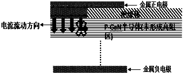
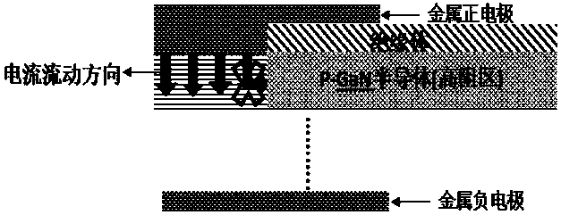
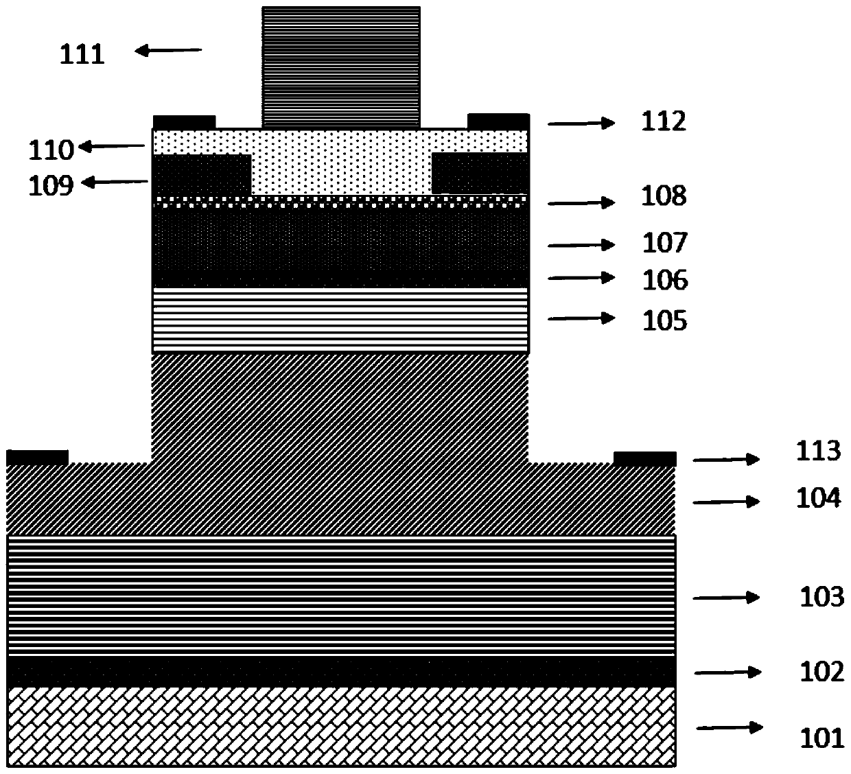
[0059] The epitaxial structure of the VCSEL device with a high dielectric constant current confinement hole in this embodiment sequentially includes a circular substrate 101, a buffer layer 102, a nitride epitaxial DBR103 and an N-type semiconductor transmission layer 104 along the epitaxial growth direction; , the N-type semiconductor transport layer 104 is divided into two parts, the lower layer completely covers the nitride epitaxial DBR103, with a thickness of 2 μm; the projected area of ​​the upper layer is 80% of the area of ​​the lower layer, and is the same as the center of the lower layer, and the thickness is 0.5 μm; The upper layer of the N-type semiconductor transport layer 104 is successively multi-quantum well layer 105, P-type current blocking layer 106, P-type semiconductor transport layer 107; P-type heavily doped semiconductor transport layer 108; P-type heavily doped The outer side of the upper surface of the hetero-semiconductor transport layer 108 is an ann...

Embodiment 2

[0069] The epitaxial structure of the VCSEL device with a high dielectric constant current confinement hole in this embodiment sequentially includes a circular substrate 101, a buffer layer 102, a nitride epitaxial DBR103 and an N-type semiconductor transmission layer 104 along the epitaxial growth direction; , the N-type semiconductor transport layer 104 is divided into two parts, the lower layer completely covers the nitride epitaxial DBR103, with a thickness of 2 μm; the projected area of ​​the upper layer is 80% of the area of ​​the lower layer, and is the same as the center of the lower layer, and the thickness is 0.5 μm; The upper layer of the N-type semiconductor transport layer 104 is successively multi-quantum well layer 105, P-type current blocking layer 106, P-type semiconductor transport layer 107; P-type heavily doped semiconductor transport layer 108; P-type heavily doped The outer side of the upper surface of the hetero-semiconductor transport layer 108 is an ann...


PUM


Abstract

The invention discloses a VCSEL device with a high-dielectric-constant current limiting hole and a preparation method thereof. An epitaxial structure of the device sequentially comprises a substrate, a buffer layer, a nitride epitaxial DBR and an N-type semiconductor transmission layer in the epitaxial growth direction. The N-type semiconductor transmission layer is divided into two parts, wehrein the lower layer completely covers the nitride epitaxy DBR. A multi-quantum well layer, a P-type current blocking layer and a P-type semiconductor transmission layer are sequentially arranged on the N-type semiconductor transmission layer; a P-type heavily-doped semiconductor transmission layer; and the outer side of the upper surface of the P-type heavily-doped semiconductor transmission layer is provided with an annular high-dielectric-constant insulating layer which is made of non-doped HfO2 or Ta2O5. Compared with a device with a tunneling junction, the device with the high-dielectric-constant current limiting hole has the advantages that the process time can be reduced by nearly 40%, the light-emitting threshold value can be reduced by about 0.5 mA, and the output power at the temperature of 80 mA is improved by 14.3% compared with that of a conventional device.

Description

technical field [0001] The invention relates to the field of vertical cavity surface emitting devices in semiconductor lasers, in particular to a preparation method of a VCSEL device with high dielectric constant confinement holes. Background technique [0002] The concept of vertical cavity surface emitting lasers (VCSELs) was first proposed by Professor Kenichi Iga and his colleagues in 1977, and the first device was realized in 1979. Since then, the research field of VCSELs has shown a rapid development trend, and it was soon commercialized in 1994. Now VCSEL has replaced the edge-firing laser and is used in short-distance optical fiber communication, such as Ethernet and Fiber Channel (Fibre Channel). In 2004, VCSELs were first used in an optical computer mouse. On September 13, 2017, the iPhone X was released, and the facial recognition function used VCSEL technology. After that, Apple spent 2.58 billion yuan to help Finisar increase the production of VCSEL. [0003]...

Claims


Application Information

Patent Timeline
Patent Type & Authority Applications(China)
IPC IPC(8): H01S5/183H01S5/187
CPCH01S5/18308H01S5/187
Inventor 张勇辉杭升张紫辉
Owner HEBEI UNIV OF TECH
Why Eureka
Try Eureka