
Method for polishing silicon wafer and method for manufacturing silicon wafer

A silicon wafer, double-sided polishing technology, applied in the direction of manufacturing tools, chemical instruments and methods, grinding/polishing equipment, etc., can solve the problem that silicon wafers cannot be shipped as products, and achieve the purpose of suppressing small defects such as step difference and grinding grain fixation effect

Active Publication Date: 2019-09-27
SUMCO CORP
View PDF6 Cites 0 Cited by
  • Summary
  • Abstract
  • Description
  • Claims
  • Application Information

AI Technical Summary

Problems solved by technology

On the other hand, silicon wafers that do not satisfy the above-mentioned desired criteria are judged as defective products, and such silicon wafers cannot be shipped as products.

Method used


Image

  • Method for polishing silicon wafer and method for manufacturing silicon wafer
  • Method for polishing silicon wafer and method for manufacturing silicon wafer
  • Method for polishing silicon wafer and method for manufacturing silicon wafer

Examples


Embodiment

[0087] (invention example)

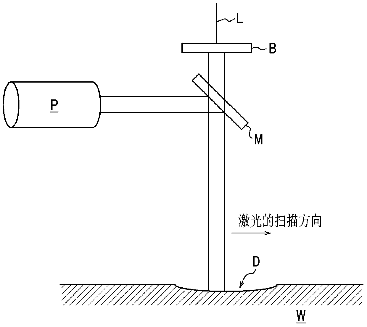
[0088] A silicon wafer is produced by the method for producing a silicon wafer based on the present invention. First, after the diameter was adjusted by grinding the outer peripheral portion of a single crystal ingot grown by the CZ method, a notch showing a orientation was formed on the outer peripheral portion of the ingot. Next, after performing the process of cutting out a block from a silicon single crystal ingot, the block in which the notch part was formed was sliced, and the silicon wafer of diameter 300mm was obtained.

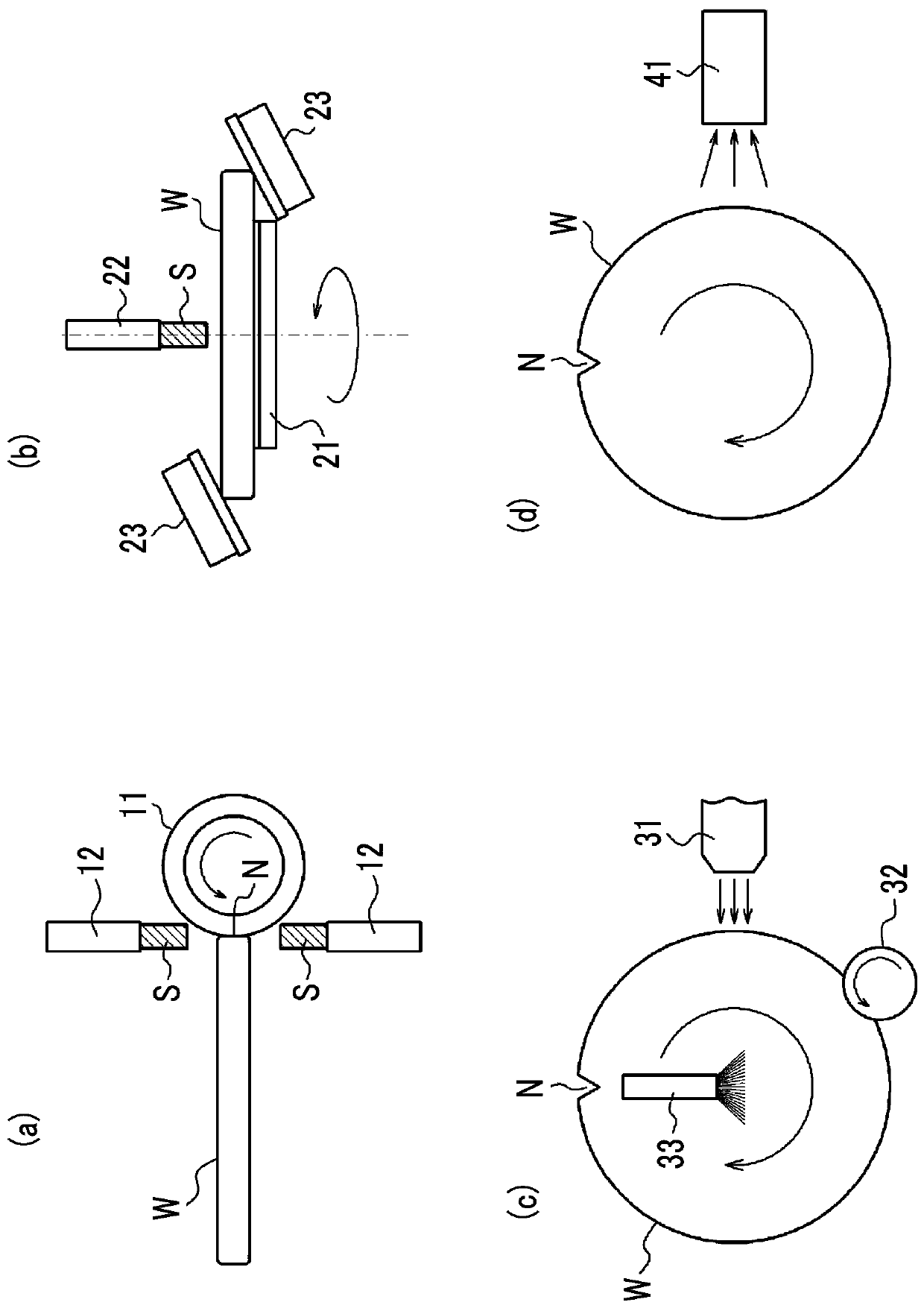
[0089] Next, a chamfering process was performed on the outer peripheral portion of the silicon wafer using a chamfering machine. Specifically, while rotating the silicon wafer, the outer peripheral portion of the wafer was pressed against a metal bond grinder having a large grain size, thereby performing primary chamfering on the outer peripheral end portion of the silicon wafer.

[0090] Next, the silicon wafer subject...


PUM


Abstract

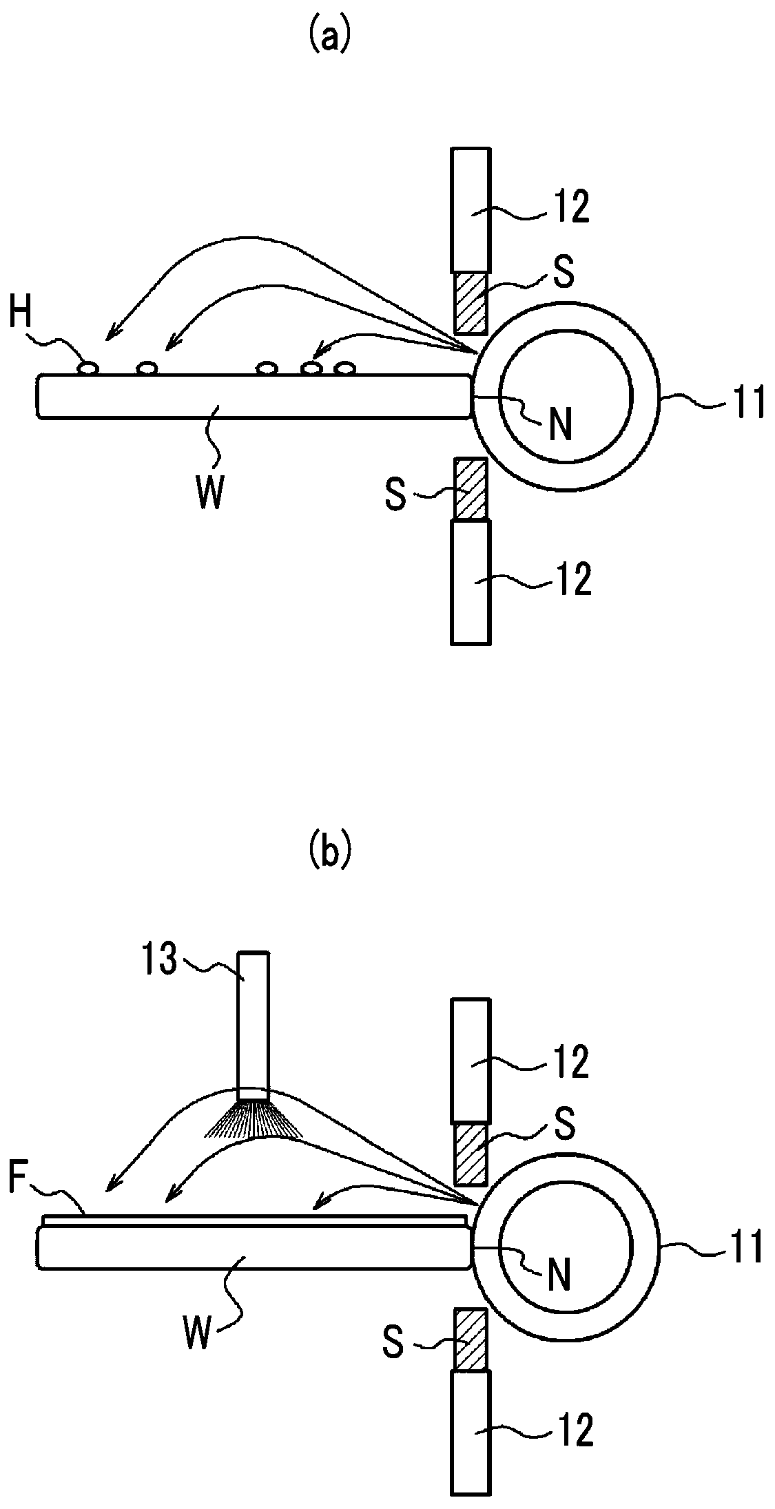
Provided are a method for polishing a silicon wafer and a method for manufacturing a silicon wafer which are capable of suppressing the occurrence of a step-shaped micro defect. This method for polishing a silicon wafer is characterized by being provided with: a double-sided polishing step for performing a polishing process on the front and rear surfaces of a silicon wafer; a notch part polishing step for polishing a chamfered section of a notch part of the silicon wafer after the double-sided polishing step; an outer peripheral chamfered section polishing step for polishing an outer peripheral chamfered section except for the chamfered section of the notch part after the notch polishing process; and a finish polishing step for finish polishing the front surface of the silicon wafer after the outer peripheral chamfered section polishing step, wherein the notch part polishing step is performed in a state in which the front surface is wet with water.

Description

technical field [0001] The invention relates to a method for polishing a silicon wafer and a method for manufacturing the silicon wafer. Background technique [0002] Conventionally, silicon wafers have been widely used as substrates of semiconductor devices. Silicon wafers were produced as follows. First, a silicon single crystal ingot is grown by the pulling (Czochralski, CZ) method or the like. Next, grinding is performed on the outer peripheral portion of the grown silicon single crystal ingot to adjust the diameter of the ingot to a predetermined value. [0003] Next, notches showing a specific crystal orientation are formed on the outer peripheral surface of the peripherally ground single crystal silicon ingot. For example, a notch showing a <110> orientation or the like is formed on a silicon wafer whose crystal plane is the (100) plane. The notch is formed, for example, by moving an appropriate grinder in the axial direction in contact with the outer periph...

Claims


Application Information

Patent Timeline
Patent Type & Authority Applications(China)
IPC IPC(8): H01L21/304B24B1/00B24B9/00B24B37/08
CPCB24B1/00B24B9/00B24B37/08H01L21/304B24B9/065C30B29/06C30B33/00H01L21/02021H01L21/02024H01L21/02013H01L21/02016H01L21/02052H01L21/02057C30B15/00H01L21/67288
Inventor 森田刚史
Owner SUMCO CORP
Learn More