Mass transfer device and mass transfer method

A transfer device and a mass transfer technology are applied in the mass transfer device and the field of mass transfer, which can solve the problems of poor transfer alignment accuracy and low work efficiency, and achieve the effect of improving work efficiency.

Active Publication Date: 2019-10-11
BOE TECH GRP CO LTD
View PDF6 Cites 7 Cited by
  • Summary
  • Abstract
  • Description
  • Claims
  • Application Information

AI Technical Summary

Problems solved by technology

In this way, each Micro-LED chip on the wafer needs to be cut individually, and then arranged on the blue film according to the required pitch size on the integ...

Method used


Image

  • Mass transfer device and mass transfer method
  • Mass transfer device and mass transfer method
  • Mass transfer device and mass transfer method

Examples


Embodiment Construction

[0057] The following will clearly and completely describe the technical solutions in the embodiments of the present invention with reference to the accompanying drawings in the embodiments of the present invention. Obviously, the described embodiments are some of the embodiments of the present invention, but not all of them. Based on the embodiments of the present invention, all other embodiments obtained by persons of ordinary skill in the art without creative efforts fall within the protection scope of the present invention.

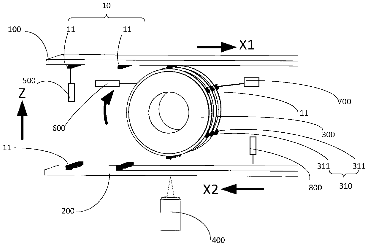
[0058] In order to more clearly describe the mass transfer device and the mass transfer method for micro components provided by the embodiments of the present invention in detail, the related prior art will be described below.

[0059] In the prior art, taking Micro-LED as an example, a CMOS integrated circuit process can be used to manufacture a driving circuit to realize a display technology for addressing control and individual driving of each pixel....


PUM


Abstract

The invention provides a mass transfer device and a mass transfer method. The mass transfer device comprises a first bearing platform; a second bearing platform which bears a target substrate and is opposite to the first bearing platform; a roller which is arranged between the first bearing platform and the second bearing platform, wherein a rotating shaft of the roller is parallel to the bearingsurface of the first bearing platform, a plurality of groups of pickup units are arranged on the outer peripheral surface of the roller at intervals in the circumferential direction, each group of pickup units comprises a plurality of pickup points which are arranged at intervals in the axial direction of the roller, and the distance between every two adjacent pickup points in the same group of pickup units in the axial direction of the roller is greater than the distance between the micro elements on the first bearing table. The first bearing platform translates in a first direction relativeto the roller, wherein the first direction is the rotating tangent direction of the roller at the contact point of the peripheral surface of the roller and the first bearing surface; the second bearing platform translates in the direction opposite to the first direction relative to the roller. According to the invention, the mass transfer working efficiency of the micro-elements is improved, the transfer alignment precision is high, and the product yield is high.

Description

technical field [0001] The invention relates to the technical field of semiconductor display, in particular to a mass transfer device and a mass transfer method. Background technique [0002] Micro-LED (miniature light-emitting diode) is to miniaturize and matrix the traditional LED (light-emitting diode) structure, and use CMOS (Complementary Metal Oxide Semiconductor, Complementary Metal Oxide Semiconductor) integrated circuit technology to make a driving circuit to realize Each pixel is addressable and individually driven display technology. Since the brightness, life, contrast, response time, energy consumption, viewing angle and resolution of Micro-LED technology are stronger than those of LCD and OLED technology, plus it is self-illuminating, simple in structure, small in size and energy-saving. The advantages of the display technology have been regarded as the next generation of display technology by many manufacturers and have begun to actively lay out. [0003] On...

Claims


Application Information

Patent Timeline
IPC IPC(8): H01L21/67H01L21/78H01L27/15H01L33/48
CPCH01L21/67144H01L21/78H01L27/156H01L33/48H01L2933/0033
Inventor 闫俊伟李丽高浩然
Owner BOE TECH GRP CO LTD
Why Eureka
Try Eureka