Perovskite type electroluminescent device and preparation method thereof

An electroluminescent device, perovskite-type technology, applied in the fields of electro-solid devices, semiconductor/solid-state device manufacturing, electrical components, etc., can solve the problem of unbalanced injection and transport of electrons and holes, and improve the probability of injection and transport , The effect of improving external quantum conversion efficiency and high specific surface area

Inactive Publication Date: 2019-10-18
SHENZHEN CHINA STAR OPTOELECTRONICS SEMICON DISPLAY TECH CO LTD
View PDF4 Cites 2 Cited by
  • Summary
  • Abstract
  • Description
  • Claims
  • Application Information

AI Technical Summary

Problems solved by technology

[0006] An object of the present invention is to provide a perovskite-type electroluminescent device, which can solve the problem of unbalanced injection and transport of electrons and holes in perovskite light-emitting devices in the prior art

Method used


Image

  • Perovskite type electroluminescent device and preparation method thereof
  • Perovskite type electroluminescent device and preparation method thereof

Examples


Embodiment 1

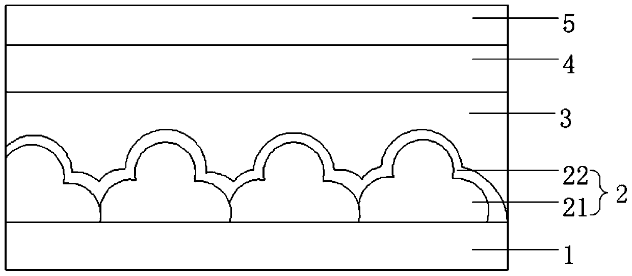
[0031] This embodiment provides a perovskite electroluminescence device, please refer to figure 1 , figure 1 Shown is a schematic cross-sectional view of the perovskite electroluminescent device provided in this embodiment, including an anode layer 1 , a hole transport layer 2 , a light emitting layer 3 , an electron transport layer 4 and a cathode layer 5 arranged in sequence. The hole transport layer 2 is disposed on the anode layer 1 , the light emitting layer 3 is disposed on the hole transport layer 2 , the electron transport layer 4 is disposed on the light emitting layer 3 , and the cathode layer 5 is disposed on the electron transport layer 4 .

[0032] In specific implementation, the anode layer 5 can be made of indium tin oxide (ITO, Indium Tin Oxides) or indium zinc oxide (IZO, Idium Zinc Oxides) or indium gallium zinc oxide (IGZO, Indium Gallium Zinc Oxides), etc., here No limit.

[0033] The light-emitting layer 3 is a light-emitting material with a perovskite s...

Embodiment 2

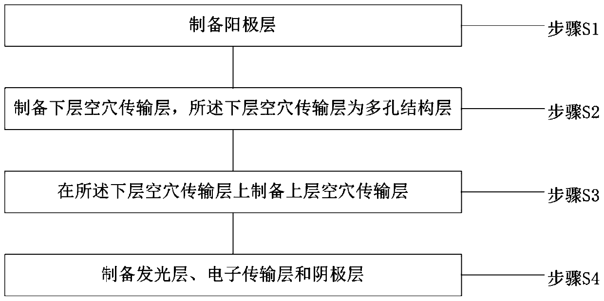
[0039] This embodiment provides a method for preparing the perovskite-type electroluminescent device described in Embodiment 1, please refer to figure 2 , figure 2 Shown is the flowchart of the preparation method of the perovskite-type electroluminescent device provided in this embodiment, including the following steps:

[0040] Step S1: preparing an anode layer;

[0041] Step S2: preparing the lower hole transport layer, the lower hole transport layer is a porous structure layer;

[0042] Methods for preparing the lower hole transport layer include spin coating, etching or printing.

[0043] Step S3: preparing an upper hole transport layer on the lower hole transport layer;

[0044]The lower hole transport layer is annealed first, and then the upper hole transport layer is prepared. The method for preparing the upper hole transport layer includes spin coating, evaporation or sputtering.

[0045] Step S4: Prepare the light-emitting layer, the electron transport layer and...


PUM


Abstract

The invention provides a perovskite type electroluminescent device and a preparation method thereof; the perovskite type electroluminescent device comprises a hole transport layer and a light-emittinglayer in sequence, wherein the light-emitting layer is arranged on the hole transport layer; the hole transport layer comprises an upper hole transport layer and a lower hole transport layer, whereinthe lower hole transport layer is a porous structure layer; and the upper hole transport layer adopts a material of a traditional hole transport layer, and the hole transport layer composed of the material and the porous structure layer has a high specific surface area, so that the interface contact area between the hole transport layer and the light-emitting layer can be effectively increased, the hole injection and transmission rate is improved, the injection and transportation balance of electrons and holes is facilitated, and the external quantum conversion efficiency of the perovskite light-emitting device is further improved.

Description

technical field [0001] The invention relates to the technical field of display panels, in particular to a perovskite electroluminescence device and a preparation method thereof. Background technique [0002] Perovskite materials (ABX 3 ) has the characteristics of excellent photoelectric properties, adjustable band gap, solution preparation, and low cost, wherein A is methylamine (MA+), formamidine (FA+), cesium (Cs+) or organic macromolecules, etc., and B is lead ( Pb2+), tin (Sn2+), etc., X is halogen chlorine (Cl-), bromine (Br-), iodine (I-) and the like. At present, the photoelectric conversion efficiency of perovskite materials in the field of solar cells has reached 23.7%, surpassing that of traditional silicon-based solar cells. At the same time, its stability problem is gradually being solved, and it has considerable commercial prospects. [0003] The application of perovskite materials in the display field (PeLED) followed closely behind. After just four years of...

Claims


Application Information

Patent Timeline
Patent Type & Authority Applications(China)
IPC IPC(8): H01L51/50H01L51/56
CPCH10K50/156H10K71/00H10K50/11H10K85/50H10K50/135
Inventor 江沛李佳育徐君哲陈书志
Owner SHENZHEN CHINA STAR OPTOELECTRONICS SEMICON DISPLAY TECH CO LTD
Why Eureka
Try Eureka