Amphoteric molecule modified perovskite photovoltaic device and preparation method and application thereof

A technology of amphiphilic molecules and photovoltaic devices, which is applied in semiconductor/solid-state device manufacturing, photovoltaic power generation, electric solid-state devices, etc.

Active Publication Date: 2020-06-02
THE NAT CENT FOR NANOSCI & TECH NCNST OF CHINA
View PDF7 Cites 4 Cited by
  • Summary
  • Abstract
  • Description
  • Claims
  • Application Information

AI Technical Summary

Problems solved by technology

However, the surface defects of the perovskite active layer in perovskite optoelectronic materials and the transport of electrons and holes in perovskite devices are still the key factors restricting their photoelectric conversion efficiency and device stability.

Method used


Image

  • Amphoteric molecule modified perovskite photovoltaic device and preparation method and application thereof
  • Amphoteric molecule modified perovskite photovoltaic device and preparation method and application thereof
  • Amphoteric molecule modified perovskite photovoltaic device and preparation method and application thereof

Examples


preparation example Construction

[0054] The preparation method of the present invention will be further described in detail in conjunction with specific examples below. It should be understood that the following examples are only for illustrating and explaining the present invention, and should not be construed as limiting the protection scope of the present invention. All technologies realized based on the above contents of the present invention are covered within the scope of protection intended by the present invention.

[0055] The experimental methods used in the following examples are conventional methods unless otherwise specified; the reagents and materials used in the following examples can be obtained from commercial sources unless otherwise specified.

Embodiment 1

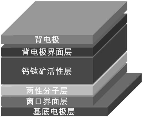
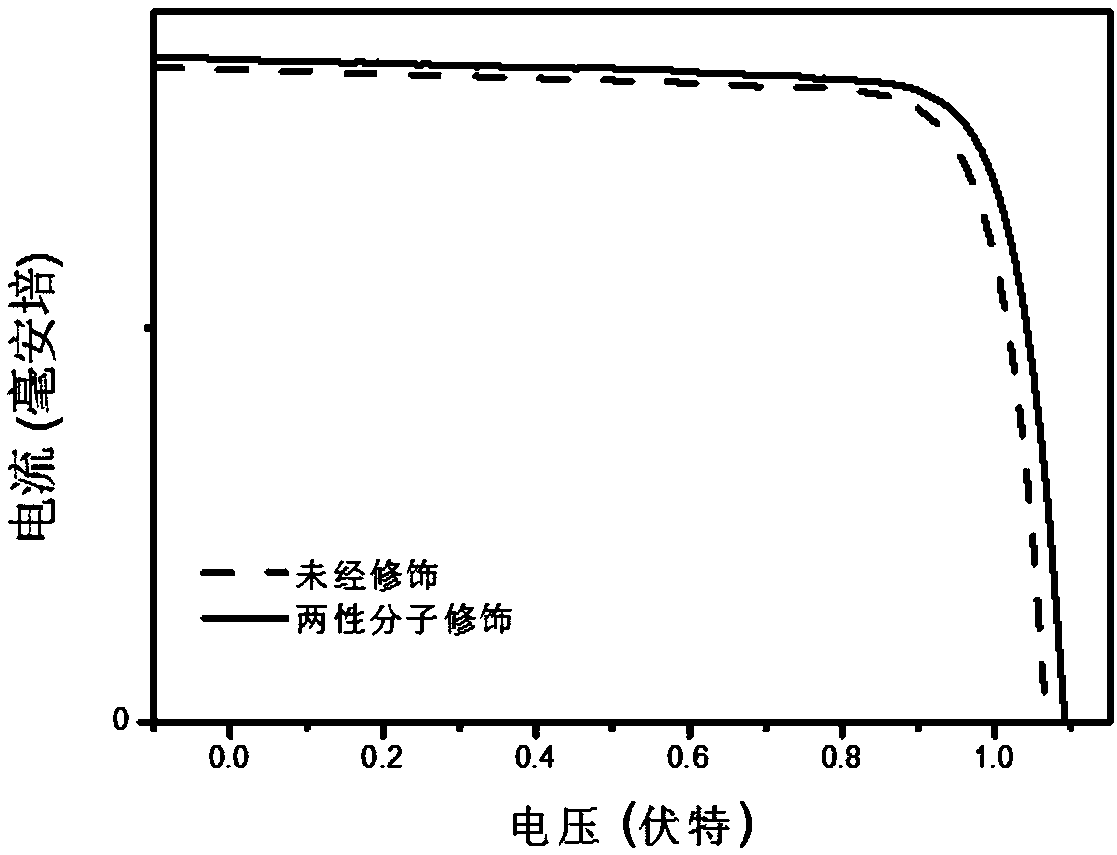
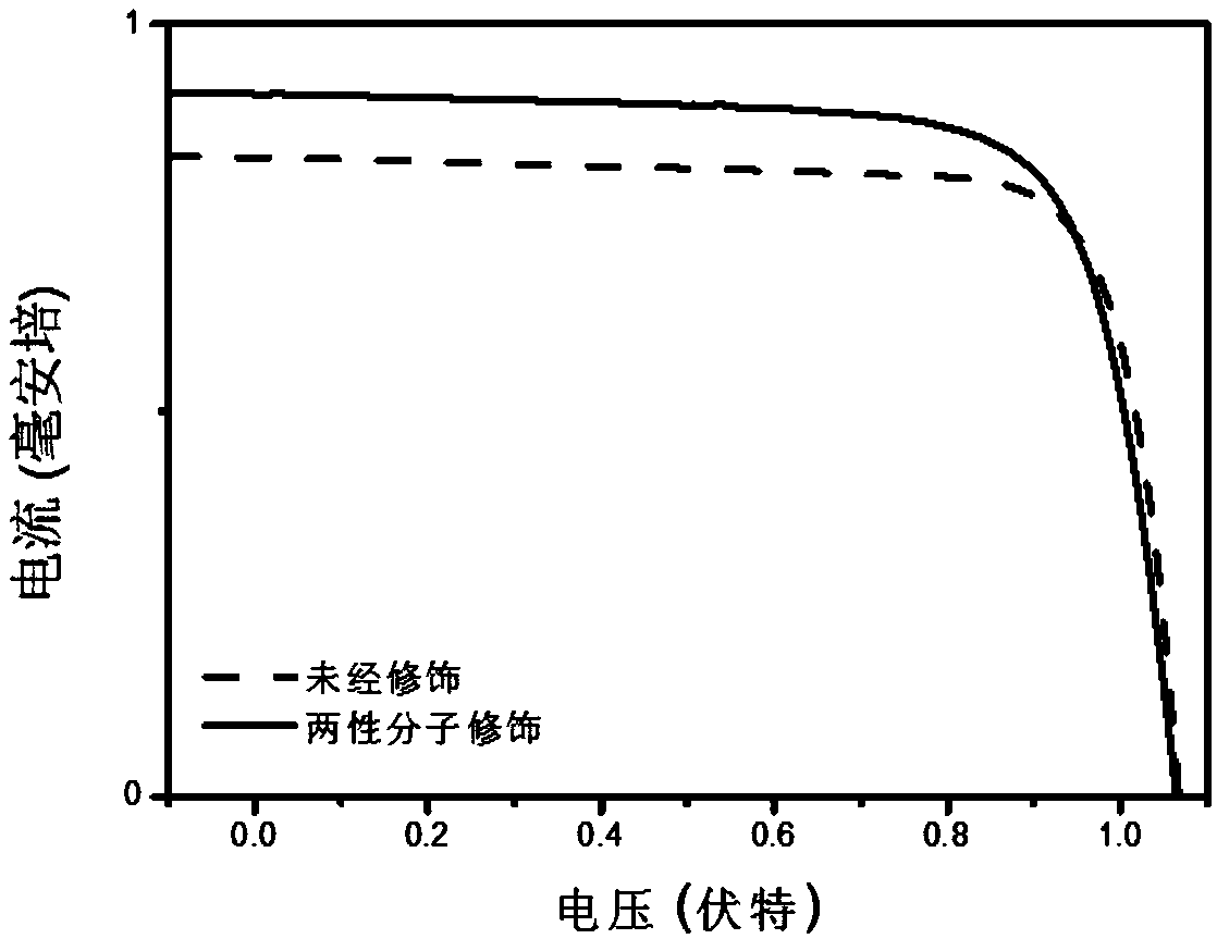
[0057] The invention provides a perovskite photovoltaic device modified by amphiphilic molecules and a preparation method thereof, comprising the following steps:

[0058] (1) Using ITO conductive glass (thickness 50nm) as the substrate, spin-coat 0.5mg / mL P3CTS aqueous solution on the ITO conductive glass, the spin-coating speed is 1000rpm, the spin-coating time is 10s, and anneal at 100°C for 10min after the spin-coating is completed , the thickness of the P3CTS layer is 20nm;

[0059] (2) Spin-coat 0.5mg / mL AMPS aqueous solution on the ITO-P3CTS obtained in step (1), the spin-coating speed is 1000rpm, and the spin-coating time is 10s. 10nm;

[0060] (3) Add 0.5M CH 3 NH 3 PB 3 The perovskite solution is spin-coated on the ITO-P3CTS-AMPS obtained in step (2), the spin-coating speed is 1000rpm, the spin-coating time is 10s, after the spin-coating is completed, anneal at 60°C for 5min, and the thickness of the perovskite layer is 400nm;

[0061] (4) spin coating 5mg / mL PC...

Embodiment 2

[0066] The invention provides a perovskite photovoltaic device modified by amphiphilic molecules and a preparation method thereof, comprising the following steps:

[0067] (1) Using ITO conductive glass (thickness 200nm) as the substrate, spin-coat 1mg / mL P3CTS aqueous solution on the ITO conductive glass, the spin-coating speed is 3000rpm, the spin-coating time is 20s, and anneal at 150°C for 20min after the spin-coating is completed. The thickness of the P3CTS layer is 50nm;

[0068] (2) Spin-coat 6mg / mL ADPS aqueous solution on the ITO-P3CTS obtained in step (1), the spin-coating speed is 3000rpm, the spin-coating time is 20s, after the spin-coating is completed, anneal at 150°C for 15min, and the thickness of the ADPS layer is 5nm;

[0069] (3) Add 1M CH3 NH 3 PB 3 The perovskite solution is spin-coated on the ITO-P3CTS-ADPS obtained in (2), the spin-coating speed is 3000rpm, the spin-coating time is 20s, after the spin-coating is completed, anneal at 100°C for 10min, a...


PUM

PropertyMeasurementUnit
thicknessaaaaaaaaaa
thicknessaaaaaaaaaa
thicknessaaaaaaaaaa

Abstract

The invention discloses an amphoteric molecule modified perovskite photovoltaic device and a preparation method and application thereof. The invention relates to amphoteric molecules, an amphoteric molecule interface modification layer is introduced into a perovskite photovoltaic device interface layer; the perovskite photoactive layer in the perovskite photovoltaic device is modified to passivatethe surface defects of the perovskite photoactive layer and improve the transmission efficiency of electrons and holes at the interface of the device, so that the perovskite photovoltaic device withhigh photoelectric conversion efficiency and high stability is realized. The interface defects in the perovskite photovoltaic device are passivated. The amphoteric molecule modified perovskite photovoltaic device prepared by adopting the method is environment-friendly and low in energy consumption.

Description

technical field [0001] The invention belongs to the field of photovoltaic device materials, and relates to a perovskite photovoltaic device modified by amphiphilic molecules, a preparation method and application thereof. Background technique [0002] A semiconductor is a special material between a conductor and an insulator. Under a certain light or voltage, the electrons in it can be excited from a bound state to a freely moving state, thereby realizing photoelectric energy conversion, showing Excellent photoelectric performance. Semiconductor optoelectronic devices play an important role in energy shortage issues, sustainable development, and new electronic devices. From the 1950s to the present, silicon-based solar cells, a semiconductor material, have moved from laboratories to applications, occupying the main market of solar cells and corresponding optoelectronic devices. However, the preparation process of silicon-based photoelectric materials is cumbersome, the cost...

Claims


Application Information

Patent Timeline
Patent Type & Authority Applications(China)
IPC IPC(8): H01L51/42H01L51/44H01L51/48
CPCH10K71/12H10K30/10H10K30/80Y02E10/549
Inventor 冷炫烨周惠琼唐智勇
Owner THE NAT CENT FOR NANOSCI & TECH NCNST OF CHINA
Why Eureka
Try Eureka