Blue film, manufacturing method and electronic product
A production method, the technology of blue film, applied in the field of decorative film, can solve the problems of singleness, poor product texture, poor durability of decorative film, etc., and achieve the effect of not being easy to damage, long service life, and meeting the needs of the market
- Summary
- Abstract
- Description
- Claims
- Application Information
AI Technical Summary
Problems solved by technology
Method used
Image
Examples
Embodiment 1
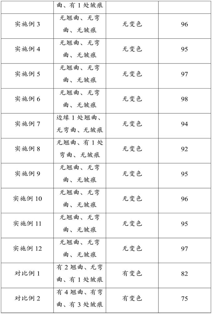
[0043] A blue film, including a glass substrate, a first silicon oxide film layer, a first silicon film layer, a second silicon oxide film layer, a second silicon film layer, and a third silicon oxide film layer, and a third silicon oxide film layer.
[0044] Among them, the first silicon oxide film layer thickness is 2 nm, the first silicon film layer thickness is 25 nm, and the second silicon oxide film layer thickness is 74 nm, and the second silicon film layer thickness is 25 nm, and the third silicon oxide film layer thick is 4 nm.
Embodiment 2
[0046] A blue film, including a glass substrate, a first silicon oxide film layer, a first silicon film layer, a second silicon oxide film layer, a second silicon film layer, and a third silicon oxide film layer, and a third silicon oxide film layer.
[0047] Among them, the first silicon oxide film layer thickness is 10 nm, the first silicon film layer thickness is 21 nm, and the second silicon oxide film layer thickness is 65 nm, the second silicon film layer thickness is 21 nm, and the third silicon oxide film layer thickness is 1 nm.
[0048] Embodiment 1 and Embodiments of each membrane layer in Example 2 are not within the preferred thickness range of the present invention.
Embodiment 3
[0050] A blue film, including a glass substrate, a first silicon oxide film layer, a first silicon film layer, a second silicon oxide film layer, a second silicon film layer, and a third silicon oxide film layer, and a third silicon oxide film layer.
[0051] Among them, the first silicon oxide film layer is 8 nm, the first silicon film layer thickness is 23 nm, the second silicon oxide film layer thickness is 72 nm, the second silicon film layer thickness is 23 nm, and the third silicon oxide film layer thickness is 2 nm.
PUM
| Property | Measurement | Unit |
|---|---|---|
| thickness | aaaaa | aaaaa |
| thickness | aaaaa | aaaaa |
| thickness | aaaaa | aaaaa |
Abstract
Description
Claims
Application Information


