Exposure method and manufacturing method of semiconductor device

An exposure method and a technology to be exposed, which are applied in the field of photolithography and can solve the problems of affecting the inter-field magnification of overlay and increasing the error of overlay

Active Publication Date: 2019-10-22
SHANGHAI MICRO ELECTRONICS EQUIP (GRP) CO LTD
View PDF6 Cites 6 Cited by
  • Summary
  • Abstract
  • Description
  • Claims
  • Application Information

AI Technical Summary

Problems solved by technology

That is, the temperature of the silicon wafer is T2 during exposure, and its temperature is T1 when the silicon wafer is aligned. The deformation of the silicon wafer in the two scenarios will affect the inter-field magnification of the overlay, thereby increasing the overlay error.

Method used


Image

  • Exposure method and manufacturing method of semiconductor device
  • Exposure method and manufacturing method of semiconductor device
  • Exposure method and manufacturing method of semiconductor device

Examples


Embodiment 1

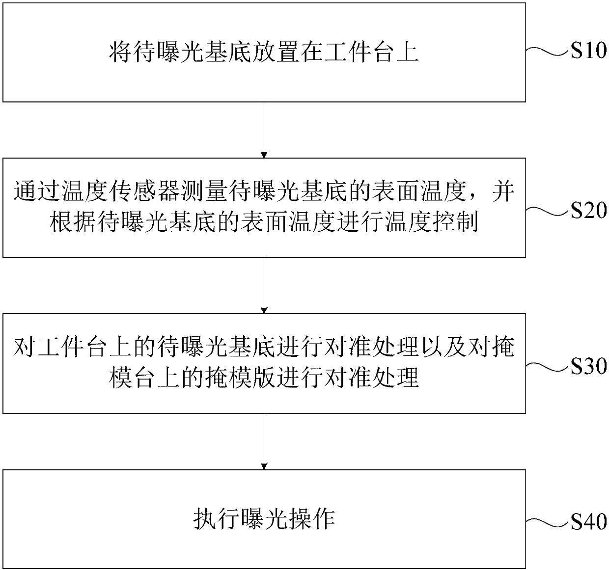
[0045] figure 1 It is a flow chart of an exposure method provided by Embodiment 1 of the present invention. see figure 1 , the exposure method provided by the embodiment of the present invention, comprising:

[0046] S10: placing the substrate to be exposed on the workpiece table.

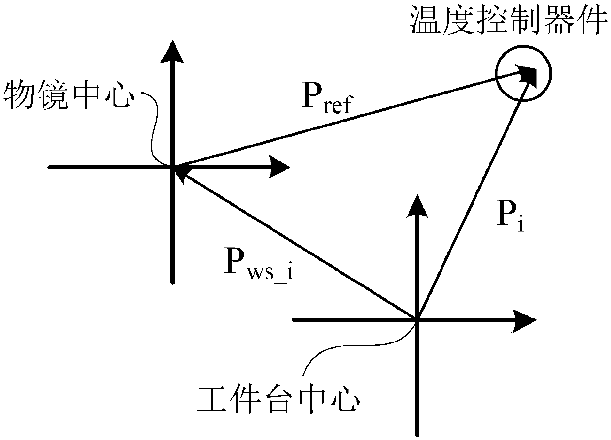
[0047] It can be understood that the workpiece table can be moved. Generally, the workpiece table can be in two positions, one is the exposure position vertically corresponding to the mask plate, which is used for exposing the substrate to be exposed, and the other is the exposure position related to the temperature. The measurement position corresponding to the sensor is used for operations such as alignment of the substrate to be exposed.

[0048] The manipulator takes out the substrate to be exposed from the film library, and first places the substrate to be exposed on the pre-alignment table for pre-alignment. After the pre-alignment of the substrate to be exposed is completed, the substrate...

Embodiment 2

[0079] This embodiment may provide an optional example based on the foregoing embodiments. On the basis of the foregoing embodiments, the exposure method includes:

[0080] S10: placing the substrate to be exposed on the workpiece table.

[0081] S20: Measure the surface temperature of the substrate to be exposed by using a temperature sensor, and perform temperature control according to the surface temperature of the substrate to be exposed.

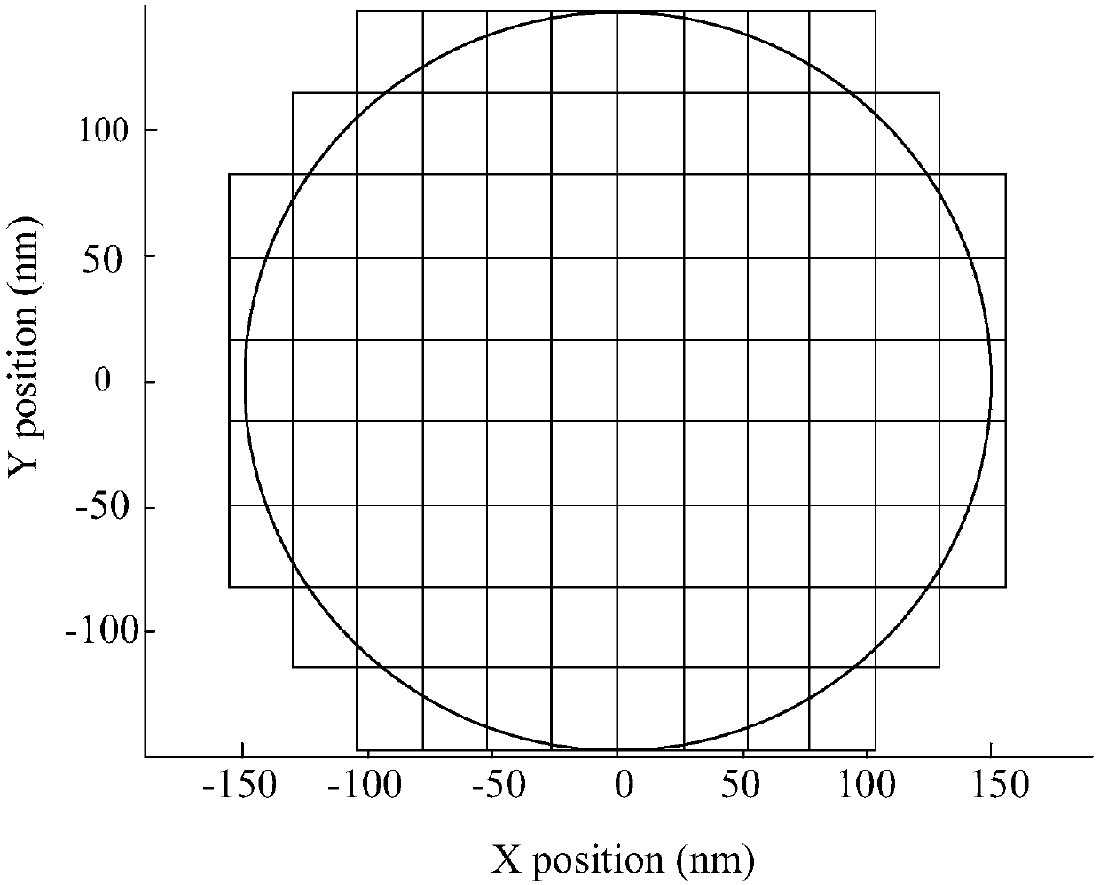
[0082] Wherein, there are many specific implementation methods for this step, and typical examples will be described in detail below, but this does not constitute a limitation to the present application. When the surface of the substrate to be exposed is divided into multiple temperature control fields, optionally, S20 includes:

[0083] First, the surface temperature of the temperature control field of the substrate to be exposed is sequentially measured according to a first preset path, and the temperature control field of the tempe...

Embodiment 3

[0106] Embodiment 3 of the present invention provides a method for manufacturing a semiconductor device including the exposure method provided by the above embodiments.

[0107] In the manufacturing method of the semiconductor device, during the exposure process of the semiconductor device, the exposure method provided in the above-mentioned embodiments is used for exposure, and the substrate to be exposed is controlled between the alignment operation and the exposure operation by controlling the surface temperature of the substrate to be exposed. The temperature difference is reduced and the time difference is shortened, which avoids problems such as deformation of the substrate to be exposed caused by too long time difference and large temperature difference, and improves the accuracy of exposure of the substrate to be exposed.


PUM


Abstract

The invention provides an exposure method and a manufacturing method of a semiconductor device. The exposure method comprises the steps of: putting a substrate to be exposed on a workpiece table; measuring the surface temperature of the substrate to be exposed by a temperature sensor, and performing temperature control according to the surface temperature of the substrate to be exposed; performingaligning processing for the substrate to be exposed on the workpiece table, and performing aligning processing for a mask on a mask platform; and executing exposure operation. According to the technical scheme provided by the invention, the substrate to be exposed is subjected to temperature control to reduce the temperature difference of the substrate to be exposed between the aligning operationand the exposure operation so as to avoid the problems of the deformation of the substrate to be exposed caused by too large temperature difference and improve the accuracy when the substrate to be exposed is exposed.

Description

technical field [0001] Embodiments of the present invention relate to photolithography technology, and in particular to an exposure method and a manufacturing method of a semiconductor device. Background technique [0002] Photolithography is a major process in the production of planar transistors and integrated circuits. As the requirements for photolithography technology become higher and higher, it is necessary to reduce errors generated during the photolithography exposure process. [0003] Overlay is one of the three major indicators of lithography machines. With the advancement of nodes, the requirements for overlay indicators are getting higher and higher, and more and more errors need to be considered, which must be considered in the indicator budget. In the lithography machine, after the silicon wafer is taken out from the external environment, it is first placed on the pre-alignment table for pre-alignment, and then placed on the workpiece table (internal environm...

Claims


Application Information

Patent Timeline
Patent Type & Authority Applications(China)
IPC IPC(8): G03F7/20G03F9/00
CPCG03F7/70875G03F9/7023
Inventor 唐彩红
Owner SHANGHAI MICRO ELECTRONICS EQUIP (GRP) CO LTD
Why Eureka
Try Eureka