Multi-step printed circuit board differential through hole processing method and printed circuit board thereof

A technology for printed circuit boards and processing methods, applied in the directions of printed circuit manufacturing, printed circuits, printed circuits, etc., can solve the problem of difficult to process multi-level printed circuit boards, etc., achieve flexible control of surface copper thickness, and reduce surface copper. Influence of unevenness, effect of improving process reliability

Inactive Publication Date: 2019-11-05
BOMIN ELECTRONICS CO LTD
View PDF7 Cites 2 Cited by
  • Summary
  • Abstract
  • Description
  • Claims
  • Application Information

AI Technical Summary

Problems solved by technology

[0010] An object of the present invention is to provide a method for processing differentiated through-holes of multi-level printed circuit boards, so as to solve the problem that it is difficult to process multi-level through-holes containing three kinds of differentiated through-holes suitable for fine circuit production with thinner surface copper in the prior art. Technical problems of printed circuit boards

Method used


Image

  • Multi-step printed circuit board differential through hole processing method and printed circuit board thereof
  • Multi-step printed circuit board differential through hole processing method and printed circuit board thereof
  • Multi-step printed circuit board differential through hole processing method and printed circuit board thereof

Examples


Embodiment 1

[0051] The method for processing differentiated through-holes of multi-level printed circuit boards provided by Embodiment 1 of the present invention can be used to process three-level printed circuit boards having three kinds of differentiated through-holes with different hole copper thicknesses.

[0052] In this embodiment, the lamination process can be used to process the laminated board in advance, and the laminated board can include two outer metal layers (that is, the surface copper foil layer, referred to as the surface copper layer) on both sides and at least one inner layer in the middle. Layer circuit layers, and an insulating dielectric layer between the inner circuit layers of each layer, and between the inner circuit layer and the outer metal layer. The method of this embodiment is applicable to circuit boards whose final surface copper thickness is 2 ounces (OZ, 1 OZ is approximately equal to 35 μm) or above 2 OZ.

[0053] In this embodiment, when initially press...

Embodiment 2

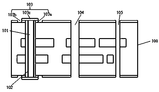
[0083] refer to Figure 9 , the embodiment of the present invention provides a printed circuit board, the initial thickness of the surface copper of the circuit board is F 0 Oz, after the first copper immersion electroplating, surface copper minus copper, second copper immersion electroplating, first electroplating, and third copper immersion electroplating, the surface copper (F) of the laminate is thickened to greater than 2OZ and less than Equal to 3OZ; where F= F 0 +ΔF 1 -ΔF 2 +ΔF 3 +ΔF 4 +ΔF 5 ; The circuit board is provided with three kinds of differentiated through holes: the first large through hole 101, the second middle through hole 104 and the third small through hole 105 along the direction vertical to the board surface; the aperture of the first large through hole 101 is larger than the Describe the aperture of the second middle through hole 104; The aperture of the second middle through hole 104 is greater than the aperture of the third small through hole 1...


PUM

PropertyMeasurementUnit
Thicknessaaaaaaaaaa
Thicknessaaaaaaaaaa

Abstract

The invention discloses a multi-step printed circuit board differential through hole processing method and a printed circuit board thereof. The problem that multi-through hole copper differentiation and a uniform copper printed circuit board are difficultly processed in the prior art is solved. According to the technical points, a first large through hole is processed in a laminate, and hole copper with the thickness of h10 is formed on the hole wall; an isolation structure is arranged around the opening of the first large through hole, so that the hole copper of the first large through hole and the surface copper of the laminate are insulated and isolated; copper reduction is carried out on the surface copper of the laminate, and then a second intermediate through hole and a third small through hole are processed; hole copper with the thickness of h20 and h30 is formed on the hole walls of the second intermediate through hole and the third small through hole; after the third small through hole is covered and plated, the hole copper of the second intermediate through hole is thickened to h21; an isolation dry film is removed for electroless copper plating, and the hole copper of the first large through hole, the second intermediate through hole and the third small through hole is thickened to the required thicknesses H1, H2 and H3 respectively; and before the third electrolesscopper plating, H1-h10=H2-h21=H3-h30. The method provided by the invention can be used for printed circuit board fabrication.

Description

technical field [0001] The invention relates to a differential through-hole processing method for a printed circuit board, in particular to a differential through-hole processing method for a multi-stage printed circuit board and a printed circuit board thereof. Background technique [0002] With the rapid development of automotive electronics and power communication modules, the functional requirements of equipment have higher and higher requirements for printed circuit boards. Circuit boards must not only provide the necessary electrical connections and mechanical supports for electronic components, but also be used Endowed with more additional functions, thick copper printed circuit boards that can integrate power supplies, provide high current, and high reliability have gradually become popular sales products in the printed circuit industry with broad prospects. [0003] Among the current-carrying lines designed for thick copper circuit board products, it is the most com...

Claims


Application Information

Patent Timeline
IPC IPC(8): H05K3/42H05K1/11
CPCH05K1/115H05K3/429H05K2201/096
Inventor 刘根陈世金李志鹏梁鸿飞韩志伟潘湛昌陈世荣
Owner BOMIN ELECTRONICS CO LTD
Why Eureka
Try Eureka