Flexible circuit board for display panel, assembly thereof, and soldering method thereof
A technology for flexible circuit boards and display panels, which is applied to printed circuit components, electrical components to assemble printed circuits, and electrical components. Effect of reducing the risk of disconnection
- Summary
- Abstract
- Description
- Claims
- Application Information
AI Technical Summary
Problems solved by technology
Method used
Image
Examples
Embodiment 1
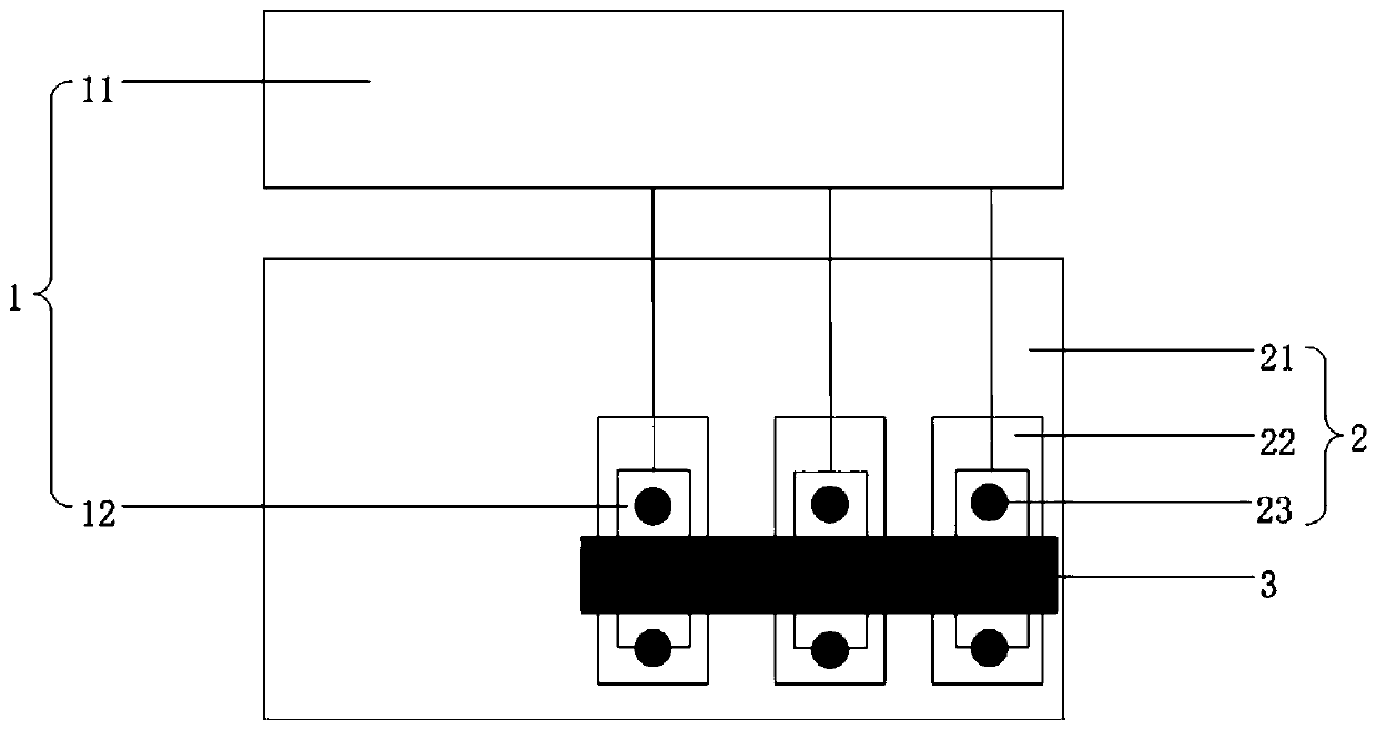
[0033] In the prior art, the backlight pins are connected to the flexible circuit board (Flexible Printed Circuit, flexible circuit board) pads, and a flat high-temperature thermocompression welding head is pressed to the surface of the flexible circuit board to make the tin on the flexible circuit board Melt, and connect the backlight module and the flexible circuit board through two tin holes on a straight line on the flexible circuit board.
[0034] During the welding process, due to the material, the unevenness of the thermal pressure head, foreign objects and other reasons, the tin coming out of the two tin holes is insufficient, there is a risk of open circuit, the welding effect cannot meet the quality requirements, and the defective rate of the product is increased. The rate directly affects the yield rate of the production line, and rework consumes manpower and material resources, which increases the manufacturing cost. In order to solve this problem, this embodiment ...
Embodiment 2
[0041] This embodiment also provides a welding method for the flexible circuit board assembly for the display panel involved in Embodiment 1, including the following steps:
[0042] Step S1: providing a backlight module 1 and a flexible circuit board 2;
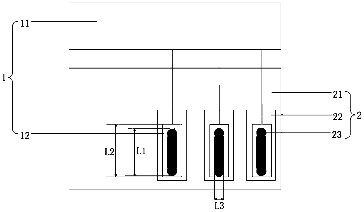
[0043] The backlight module 1 includes a backlight module body 11 and pins 12 provided on the backlight module body 11; the flexible circuit board 2 includes a flexible circuit board body 21, and the flexible circuit board body 21 is provided with a plurality of solder joints arranged in parallel and spaced apart. The pad 22 is provided with a tin slot 23 on the pad 22 .
[0044] The tin slot 23 provided in this embodiment is to connect two tin slots on a straight line on the flexible circuit board in the prior art to form the tin slot 23. The tin slot 23 is in a rectangular configuration. The diameter of the solder hole in the technology ranges from 0.2 mm to 0.3 mm. The width L3 of the solder slot in this embodiment ranges...
PUM
 Abstract
Description
Claims
Application Information


