Photoelectric detector based on InGaAs material and manufacturing method of photoelectric detector

A technology of photodetectors and light windows, which is applied in the direction of final product manufacturing, sustainable manufacturing/processing, circuits, etc., can solve the problems of affecting carrier transmission speed, complex structure, slow response speed of photodetectors, etc., and achieve improved Quantum efficiency and response speed, the effect of meeting transmission requirements

Pending Publication Date: 2019-11-12
武汉敏芯半导体股份有限公司
View PDF0 Cites 10 Cited by
  • Summary
  • Abstract
  • Description
  • Claims
  • Application Information

AI Technical Summary

Problems solved by technology

[0003] Photodetector is a light-receiving device with the function of photoelectric change. There are many types of photodetectors. In order to meet the needs of optical communication in the direction of bandwidth development, various types of high-speed photodetectors have emerged, such as avalanche photodetectors (referred to as avalanche photodetectors) APD), metal-semiconductor-metal photodetector (MSM for short), PIN photodetector, etc. APD has both detection and amplification functions, but the structure is complex; MSM does not need to manufacture pn junctions, and is combined with semiconductors that are difficult to dope It is completely compatible with the manufacturing process of electronic devices, but its performance is poor, while the PIN structure and manufacturing process are relatively simple, with excellent performance and low cost, so it is the most widely used
[0004] In particular, photodetectors using InGaAs as the absorbing material have been greatly developed. In the prior art, photodetectors using InGaAs as the absorbing material generally adopt the p-InP / i-InGaAs / n-InP structure. / i-InGaAs has a heterojunction potential barrier, which will affect the transport speed of carriers, resulting in slow response speed of existing photodetectors

Method used


Image

  • Photoelectric detector based on InGaAs material and manufacturing method of photoelectric detector
  • Photoelectric detector based on InGaAs material and manufacturing method of photoelectric detector
  • Photoelectric detector based on InGaAs material and manufacturing method of photoelectric detector

Examples


Embodiment Construction

[0032] In order to make the purpose, technical solutions and advantages of the embodiments of the present invention clearer, the technical solutions in the embodiments of the present invention will be clearly and completely described below in conjunction with the drawings in the embodiments of the present invention. Obviously, the described embodiments It is a part of embodiments of the present invention, but not all embodiments. Based on the embodiments of the present invention, all other embodiments obtained by persons of ordinary skill in the art without creative efforts fall within the protection scope of the present invention.

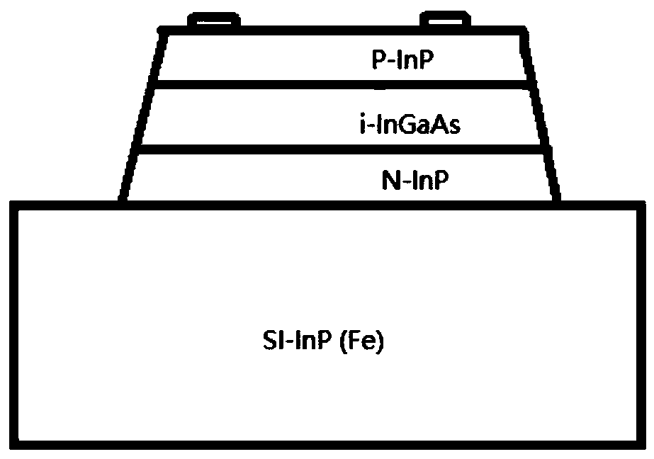
[0033] figure 1 It is a structural schematic diagram of a photodetector in the prior art, such as figure 1 As shown, Si-InP (Fe) represents the substrate, N-InP represents N-type InP, i-InGaAs represents i-type InGaAs, P-InP represents P-type InP, and the existing photodetectors are composed of substrate, N-type InP , i-type InGaAs and P-type In...


PUM

PropertyMeasurementUnit
Thicknessaaaaaaaaaa
Thicknessaaaaaaaaaa
Thicknessaaaaaaaaaa

Abstract

The embodiment of the invention provides a photoelectric detector based on an InGaAs material and a manufacturing method of the photoelectric detector. The epitaxial structure of the photoelectric detector sequentially comprises a substrate, an InP buffer layer, an N +-InGaAs contact layer, an N-type InP, an InGaAsP band gap transition layer, an InGaAs intrinsic absorption layer and a P-type dopedgradient InGaAs light window layer from the bottom to the top, wherein the concentration of an InGaAs-doped material in the P-type InGaAs light window layer is gradually changed, an N-type ohmic electrode is led out from the N-type InP layer through the N +-InGaAs contact layer, and a P-type ohmic electrode is led out from the P-type InGaAs light window layer. The embodiment of the invention provides the photoelectric detector and the manufacturing method thereof. The light window adopts an InGaAs material with gradually changed doping as a P region structure, the structure can establish a diffusion self-built electric field in the P region, and the self-built electric field effectively overcomes the self-absorption problem of photon-generated carriers, so that the quantum efficiency andthe response speed of the photoelectric detector are effectively improved, and the transmission requirement of a high-speed communication system is met.

Description

technical field [0001] The invention relates to the technical field of semiconductors, in particular to a photodetector based on InGaAs material and a manufacturing method thereof. Background technique [0002] With the gradual deepening of human information construction and the intensification of economic globalization, the number of information acquisition and exchange in all aspects of human social life is constantly increasing, and the demand for long-distance transmission of massive data and bandwidth mobile access is increasing. highlight. High-speed, ultra-high-speed optical fiber communication technology and broadband optical wireless technology have received great attention as the main methods to solve these problems. An optical fiber communication system includes optoelectronic devices such as semiconductor lasers, semiconductor detectors and optical fibers. Among them, photodetectors It is the core of the optical receiver. The optical signal is restored to the el...

Claims


Application Information

Patent Timeline
IPC IPC(8): H01L31/0304H01L31/105H01L31/18
CPCH01L31/03042H01L31/03046H01L31/105H01L31/1844Y02P70/50
Inventor 徐之韬王丹王权兵王任凡
Owner 武汉敏芯半导体股份有限公司
Why Eureka
Try Eureka