An ultraviolet-visible dual-band photodetector

A photodetector and dual-band technology, applied in circuits, electrical components, semiconductor devices, etc., can solve problems such as inability to detect, increase the complexity of device manufacturing, and narrow detection range of photodetectors

Active Publication Date: 2021-05-14
SOUTHEAST UNIV
View PDF6 Cites 1 Cited by
  • Summary
  • Abstract
  • Description
  • Claims
  • Application Information

AI Technical Summary

Problems solved by technology

[0004] Since the traditional ultraviolet photodetector and infrared photodetector can only track a single color, the detection range of the photodetector is narrow, and it is impossible to simultaneously detect the light in the ultraviolet and visible bands.
However, most of the current UV-visible dual-band detectors are mainly composed of two detectors that respond to different bands respectively. Usually, the ultraviolet and infrared detectors are connected together by metal bonding to achieve dual-band detection, which increases the Complexity of Device Fabrication

Method used


Image

  • An ultraviolet-visible dual-band photodetector

Examples


Embodiment 1

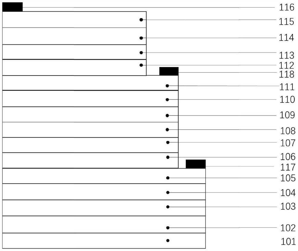
[0017] A low-temperature AlN nucleation layer 102 is grown on the C-plane sapphire by MOCVD, and the thickness of the AlN nucleation layer is 20 nm;

[0018] growing a high-temperature AlN buffer layer 103 on the low-temperature AlN nucleation layer 102, the thickness of the high-temperature AlN buffer layer being 200 nm;

[0019] A layer of n-type Al is grown on the high-temperature AlN layer 103 x1 Ga 1-x1 N buffer layer 104, Al x1 Ga 1-x1 The thickness of the N buffer layer is 300nm, using SiH 4 Doping, the doping concentration is 4×10 18 cm -3 , component x1 is 0.2;

[0020] in Al x1 Ga 1-x1 A layer of n-type Al is grown on the N buffer layer 104 x2 Ga 1-x2 N layer 105; n-type Al x2 Ga 1-x2 The thickness of the N layer 105 is 500nm, using SiH 4 Doping, where the doping concentration of Si is 2×10 18 cm -3 , Al composition x2 is 0.2;

[0021] In n-type Al x2 Ga 1-x2 A layer of non-doped i-type Al is grown on the N layer 105 x3 Ga 1-x3 N absorption layer ...


PUM

PropertyMeasurementUnit
thicknessaaaaaaaaaa
thicknessaaaaaaaaaa
thicknessaaaaaaaaaa

Abstract

The invention discloses an ultraviolet-visible dual-band photodetector, which includes a substrate layer, a low-temperature AlN nucleation layer, a high-temperature AlN buffer layer, an n-type AlGaN buffer layer, an n-type AlGaN layer, and an i-type AlGaN absorption layer arranged from bottom to top , AlGaN multiplication layer, P-type AlGaN layer, AlGaN gradient layer, n-type AlGaN layer, n-type GaN layer, InGaN multiplication layer, i-type InGaN absorption layer, P-type InGaN layer and P-type GaN layer. There is an exposed area on the side of the n-type AlGaN layer (105) and the n-type GaN layer, an n-type ohmic contact electrode is arranged on the upper surface of the exposed area, and a p-type ohmic contact layer is arranged on the upper surface of the p-type GaN. The invention can realize the detection of ultraviolet and visible light. By adjusting the Al composition of the ultraviolet absorption unit, the ultraviolet detection wavelength can be changed; by adjusting the In composition of the visible light absorption unit, the detection of blue light, green light, red light and other visible light bands can be realized. .

Description

Technical field: [0001] The invention belongs to the field of semiconductor optoelectronic devices, in particular to an ultraviolet-visible dual-band photodetector. Background technique: [0002] Gallium nitride-based semiconductor materials mainly include binary compounds GaN, InN, AlN of group III and group V elements, ternary compounds InGaN, AlGaN, AlInN and quaternary compounds AlInGaN, which have a large band gap, high thermal conductivity, and High temperature, radiation resistance, acid and alkali resistance and other characteristics, it has a wide range of application potential and good market prospects in the fields of radiation resistance, high temperature resistance, high-power microwave devices and other fields. Ternary compound Al x Ga 1-x The energy band gap of N can be adjusted by changing the Al composition x, so that the corresponding absorption wavelength is between 200 and 365 nm, and the ternary compound In x Ga 1-x The energy band gap of N (0≤x≤1) r...

Claims


Application Information

Patent Timeline
Patent Type & Authority Patents(China)
IPC IPC(8): H01L31/0304H01L31/0352H01L31/101H01L31/11
CPCH01L31/03042H01L31/03048H01L31/035272H01L31/1013H01L31/11
Inventor 庄喆李成张雄崔一平
Owner SOUTHEAST UNIV
Why Eureka
Try Eureka