Micro light-emitting element display device and manufacturing method thereof

A technology for light-emitting elements and display devices, which is applied to electrical elements, electrical solid-state devices, semiconductor devices, etc., to achieve the effects of good luminous efficiency and improved operating stability

Active Publication Date: 2019-11-22
PLAYNITRIDE DISPLAY CO LTD
View PDF7 Cites 11 Cited by
  • Summary
  • Abstract
  • Description
  • Claims
  • Application Information

AI Technical Summary

Problems solved by technology

However, in terms of the transfer accuracy of the current mass transfer technology, there is still a problem of yield when it is applied to the production of ultra-high definition (Ultra High Definition, UHD) display devices
Ev

Method used


Image

  • Micro light-emitting element display device and manufacturing method thereof
  • Micro light-emitting element display device and manufacturing method thereof
  • Micro light-emitting element display device and manufacturing method thereof

Examples


Example Embodiment

[0074] Reference will now be made in detail to the exemplary embodiments of the present invention, and examples of the exemplary embodiments are illustrated in the accompanying drawings. Whenever possible, the same reference symbols are used in the drawings and the description to indicate the same or similar parts.

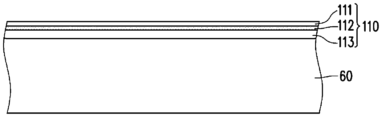
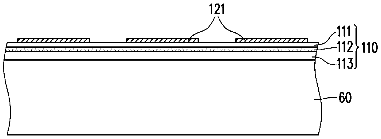
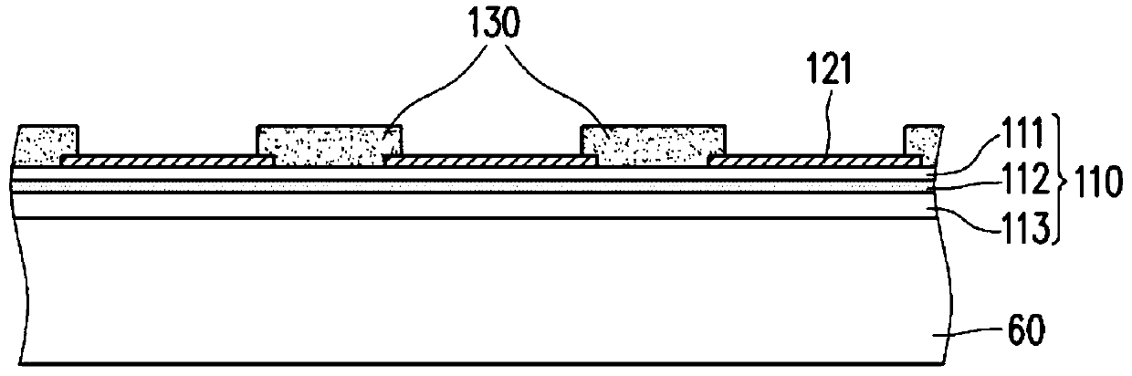
[0075] Figure 1A to Figure 1H It is a schematic cross-sectional view of the manufacturing process of the micro light emitting device display device of the first embodiment of the present invention. figure 2 Yes Figure 1H A schematic top view of the pads and shading patterns of. First, please refer to Figure 1H The micro light emitting device display device 1 includes a circuit substrate 50, a plurality of epitaxial structures 110P, and a plurality of pads 120. A plurality of epitaxial structures 110P are dispersedly arranged on the circuit substrate 50, and a plurality of pads 120 are arranged between the epitaxial structures 110P and the circuit substrate 50. Th...


PUM

PropertyMeasurementUnit
Young's modulusaaaaaaaaaa

Abstract

The invention provides a micro light-emitting element display device and a manufacturing method thereof. The micro light-emitting element display device comprises a circuit substrate, a plurality of epitaxial structures, a plurality of connecting pads and a plurality of shading patterns. The plurality of epitaxial structures are dispersedly arranged on the circuit substrate. The plurality of padsare disposed between the plurality of epitaxial structures and the circuit substrate. The plurality of epitaxial structures are electrically connected to the circuit substrate through the plurality ofpads, respectively. The plurality of shading patterns and the plurality of connecting pads are alternately arranged on the circuit substrate, and each shading pattern is connected between two adjacent connecting pads and is suitable for blocking light with the wavelength of 150nm-400nm from penetrating through.

Description

technical field [0001] The invention relates to a display device and a manufacturing method thereof, in particular to a micro light-emitting element display device and a manufacturing method thereof. Background technique [0002] In recent years, under the condition that the manufacturing cost of Organic light-emitting diode (OLED) display panels is relatively high and its service life cannot compete with the current mainstream displays, Micro LED Displays have gradually Attract the investment attention of major technology companies. In addition to the advantages of low energy consumption and long service life of materials, micro-LED display devices also have excellent optical performance, such as high color saturation, fast response speed and high contrast. [0003] At present, in the manufacturing process of micro-light-emitting element display devices, mass transfer technology plays a very important role. It transfers pre-fabricated and stored micro-light-emitting elemen...

Claims


Application Information

Patent Timeline
IPC IPC(8): H01L27/15H01L23/552H01L33/48H01L33/62
CPCH01L27/156H01L23/552H01L33/62H01L33/48H01L2933/0033H01L2933/0066
Inventor 杨翔甯吴志凌苏义闵吴柏威
Owner PLAYNITRIDE DISPLAY CO LTD
Why Eureka
Try Eureka