Organic electric luminescent device emitting white light with Improved efficiency and stability

A device and organic technology, applied in the field of organic light-emitting devices, can solve the problems of low dopant concentration and difficult process control, and achieve the effect of low driving voltage and high operational stability

Inactive Publication Date: 2002-03-20
GLOBAL OLED TECH
View PDF9 Cites 19 Cited by
  • Summary
  • Abstract
  • Description
  • Claims
  • Application Information

AI Technical Summary

Problems solved by technology

[0010] However, these OLED devices require very low dopant concentrations, making the process difficult to control when mass-manufactured

Method used


Image

  • Organic electric luminescent device emitting white light with Improved efficiency and stability
  • Organic electric luminescent device emitting white light with Improved efficiency and stability
  • Organic electric luminescent device emitting white light with Improved efficiency and stability

Examples


Embodiment 1

[0105] OLED devices were fabricated using the following methods:

[0106] The substrates coated with 80 nm ITO were sequentially ultrasonically cleaned in a commercial detergent, rinsed in deionized water, and degreased in toluene vapor. These substrates were treated with oxygen plasma for about 1 min, and plasma-assisted deposition of CHF 3 A 1 nm layer of fluorocarbon is applied. This same method was used to prepare all other devices described in this invention.

[0107] These substrates are loaded into the deposition chamber for the deposition of organic layers and cathodes.

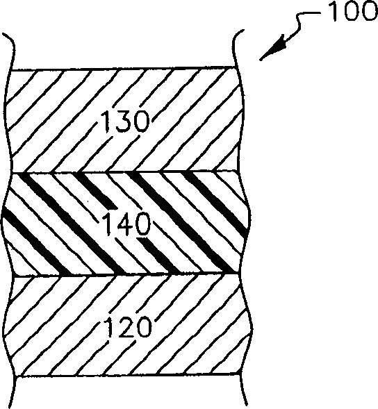
[0108] The making of device A is to deposit 150nm NPB hole transport layer (HTL) sequentially, 20nm blue light-emitting layer (EML), this layer comprises the ADN matrix containing 1.5% TBP blue dopant, 37.5nm Alq electron transport layer (ETL ), followed by 0.5 nm LiF and 200 nm Al as part of the cathode. The above process completes the deposition of the OLED device.

[0109] Then the OLED device...

Embodiment 2

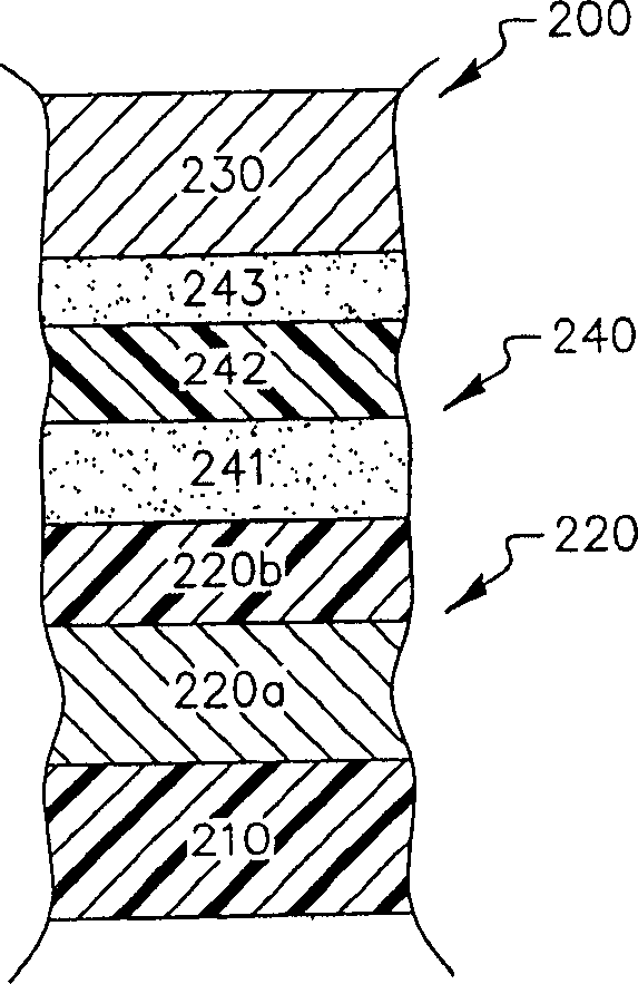
[0115] OLED devices G, H, I, J, K, and L were fabricated by inserting undoped NPB between the rubrene-doped NPB hole transport layer 341a and the blue light-emitting layer 342 .

[0116] Table 2: White OLEDs with rubrene-doped NPB HTL and blue light-emitting layer at defined positions

Device#

HTL layer

NPB undoped

layer

blue light emitting layer

electronic transmission

send layer

cathode

driving voltage

(V)

Luminous efficiency

(cd / A)

CIEx

CIE

color

G

120 nm NPB Undoped / 30 nm NPB

+1.5% rubrene doped

0 nm

20 nmADN+1.5%

TBP

35 nm Alq

200 nm MgAg

8.5

4.54

0.359

0.399

White

H

118 nm NPB undoped / 30 nm NPB+

1.5% rubrene doped

2 nm

20 nmADN+1.5%

TBP

3...

Embodiment 3

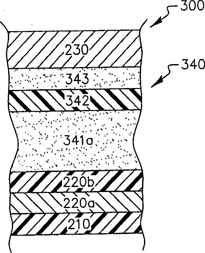
[0120] according to Figure 7 Devices M to R were fabricated with the structure shown. The deposition sequence is the same as that of device A, except that the first 20 nm Alq electron transport layer 243a is doped with different concentrations of rubrene: (M) 0.0%, (N) 0.3%, (O) 0.5%, (P ) 1%, (Q) 2%, (R) 5%. The rubrene-doped Alq layer was followed by a 15 nm undoped Alq layer 343 so that the total thickness of the rubrene-doped Alq and undoped Alq layers was equal to 37.5 nm. Device M was found to have an emission in the blue region of the electromagnetic spectrum, while the emissions of devices N and O were shifted towards blue-white. Devices P, Q and R emit white. Therefore, the Alq electron transport layer and the blue light-emitting layer doped with the optimal concentration of rubrene can generate white light.

[0121] Figure 8 EL spectra are shown for devices M to R where the concentration of rubrene in the electron transport layer was varied between 0 and 5%. ...


PUM

PropertyMeasurementUnit
thicknessaaaaaaaaaa
thicknessaaaaaaaaaa

Abstract

An organic light-emitting diode (OLED) device which produces substantially white light includes a substrate; an anode disposed over the substrate; and a hole-injecting layer disposed over the anode. The device also includes a hole transport layer disposed over the hole-injecting layer; a light-emitting layer doped with a blue light-emitting compound, disposed directly on the hole transport layer; and an electron transport layer disposed over the blue light-emitting layer. The device further includes a cathode disposed over the electron transport layer and the hole transport layer, electron transport layer, or the electron transport layer and the hole transport layer being selectively doped in a region which corresponds to an entire layer or a partial portion of a layer in contact with the blue light-emitting layer, the selective doping being with a compound which emits light in the yellow region of the spectrum.

Description

field of invention [0001] The present invention relates to organic light emitting devices (OLEDs) that produce white light. Background technique [0002] An OLED device includes a substrate, an anode, a hole transport layer made of an organic compound, an organic light-emitting layer containing a suitable dopant, an organic electron transport layer, and a cathode. OLED devices are attractive because of their low drive voltage, high brightness, wide viewing angle, and ability to have full-color planar emissive displays. Such multilayer OLED devices are described in US 4,769,292 and 4,885,211. [0003] OLED devices that efficiently produce white light are considered as low-cost replacements for several applications, such as paper-thin backlights in LCD displays, automotive blinkers, and office lighting. OLED devices that produce white light should be bright, efficient, and generally should have Committee d'Eclairage International (CIE) chromaticity coordinates of about (0.33...

Claims


Application Information

Patent Timeline
Patent Type & Authority Applications(China)
IPC IPC(8): C09K11/06G02F1/13357H01L51/00H01L51/30H01L51/50H05B33/12H05B33/14
CPCC09K2211/1011H01L51/0059C09K11/06H01L51/006H01L51/5036Y10S428/917H01L51/0054H01L51/0055H05B33/14C09K2211/1014Y02B20/181H01L51/0056H01L51/0058Y02B20/00H10K85/623H10K85/622H10K85/624H10K85/631H10K85/626H10K85/633H10K50/125
Inventor T·K·哈特瓦
Owner GLOBAL OLED TECH
Why Eureka
Try Eureka