Micro-ring delay matrix and microwave photon integrated multi-beam phased array chip and system

A microwave photonic and phased array technology, applied in optical waveguides, optics, nonlinear optics, etc., can solve the problems of beam squint, large system redundancy, large chip size, etc., to reduce chip complexity and work. The effect of compact structure and wide working bandwidth

Active Publication Date: 2019-11-26
NANJING UNIV OF AERONAUTICS & ASTRONAUTICS
View PDF1 Cites 4 Cited by
  • Summary
  • Abstract
  • Description
  • Claims
  • Application Information

AI Technical Summary

Problems solved by technology

Both schemes are based on the principle of phase shifting, and there are problems such as beam squint
In 2017, TessemaN and others realized a microwave photon integrated multi-beamforming scheme based on time-delay technology, (Tessema N, Cao Z, Van Zantvoort J H C, et al. K-band RF multi-beamformer using Si3N4TTD for home-satellitecommunications[C] / / Optical Fiber Communication Conference. Optical Society of America, 2017:Tu2I.5.) This solution uses the traditional all-pass micro-ring delay line, which only has a delay function and cannot be selected Modulates signals at different wavelengths to individually control the amplitude of signals on different elements of each beam
This solution uses a microring as a beam splitter to select signals modulated on different wavelengths, and uses a fixed delay line to delay the signal. The chip size is large, and the direction of each beam cannot be flexibly adjusted.
Although these two time-delay-based multi-beamforming schemes do not have the beam tilt effect, they either cannot control the amplitude and delay of the signal alone, and it is difficult to adjust the amplitude and beam direction of each array element signal, which greatly affects the practical application. and restrictions; or too many devices are used to achieve filtering and delay, the system redundancy is large, and the chip size is large, which is not conducive to production

Method used


Image

  • Micro-ring delay matrix and microwave photon integrated multi-beam phased array chip and system
  • Micro-ring delay matrix and microwave photon integrated multi-beam phased array chip and system
  • Micro-ring delay matrix and microwave photon integrated multi-beam phased array chip and system

Examples


Embodiment Construction

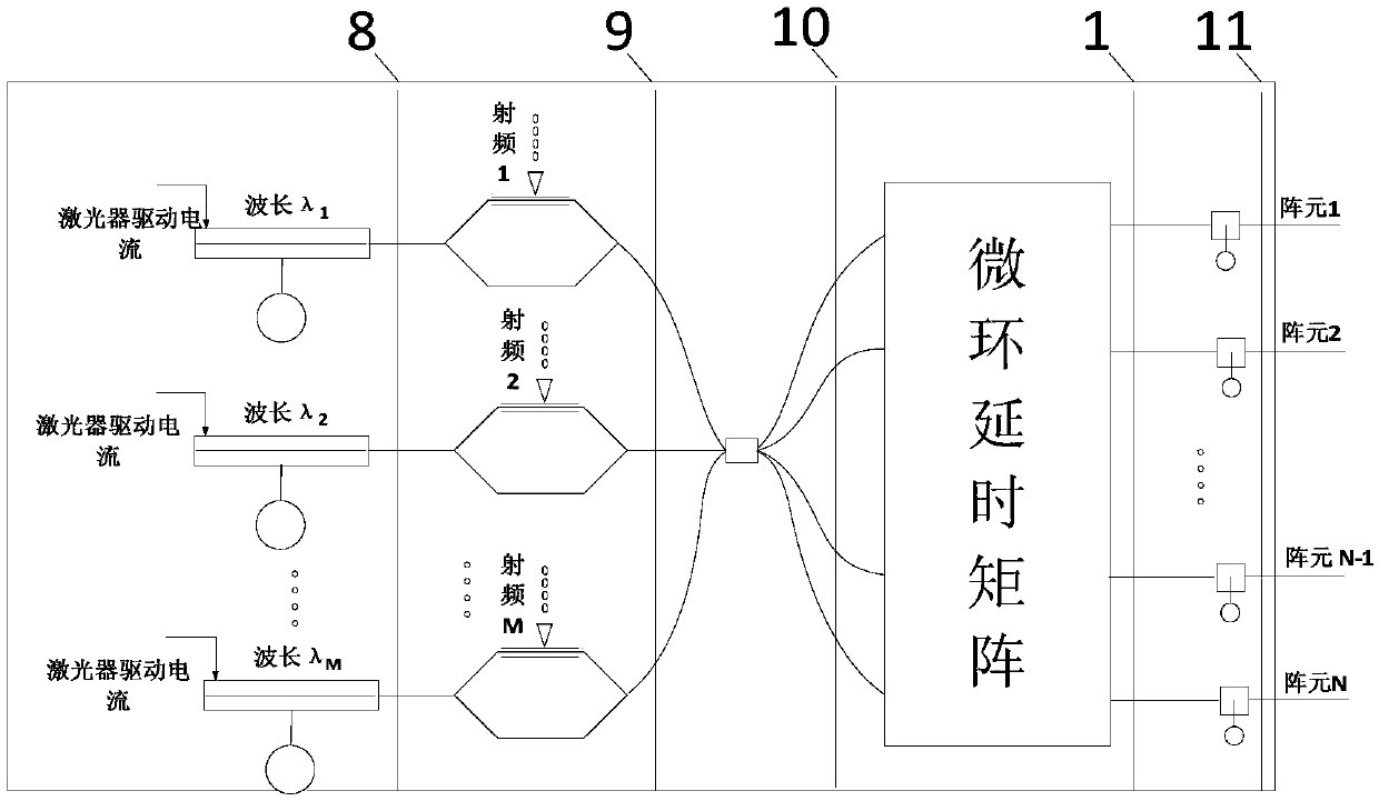
[0030]Aiming at the deficiencies of the existing microwave photonic integrated multi-beamforming scheme based on time-delay technology, the solution of the present invention is to use the upload / download micro-ring to construct the micro-ring delay matrix, and make full use of the direct part and download part of the micro-ring spectrum resources , using the filtering and delay functions of the micro-ring at the same time, thereby effectively reducing the complexity of the chip while realizing large-bandwidth adjustable multi-beam forming.

[0031] In order to facilitate the public's understanding, the technical solution of the present invention will be described in detail below in conjunction with the accompanying drawings:

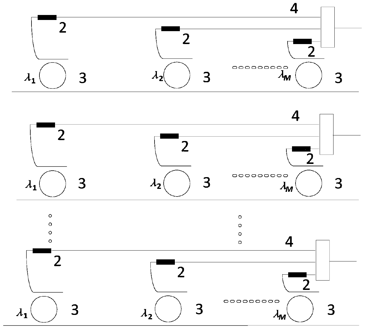
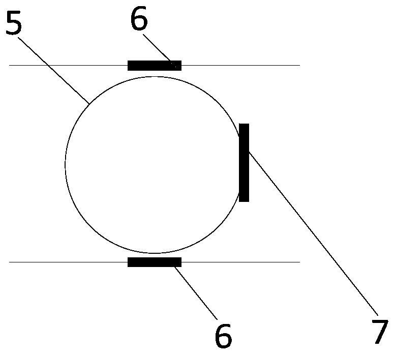
[0032] The specific structure of the microring delay matrix of the present invention is as figure 1 As shown, it has N input ports, and each input port corresponds to one row, consisting of N rows in total; each row of the microring delay matrix is ​​com...


PUM


Abstract

The invention discloses a micro-ring delay matrix. The micro-ring delay matrix comprises an array consisting of N*M upload / download (add / drop) type micro-ring units, wherein each micro-ring unit comprises at least one micro-ring resonator, an input optical waveguide, an output optical waveguide, a coupling coefficient adjusting electrode and a resonance wavelength adjusting electrode, the input optical waveguide and the output optical waveguide are respectively coupled with the micro-ring resonator, the coupling coefficient adjusting electrode is used for adjusting the coupling coefficients between the input optical waveguide and the micro-ring resonator and between the output optical waveguide and the micro-ring resonator, and the resonance wavelength adjusting electrode is used for adjusting the resonance wavelength of the micro-ring resonator. The M upload / download type micro-ring units in the same row share one input optical waveguide, and the download ends of the M upload / downloadtype micro-ring units in the same row are coupled into one path to serve as an output end of the row. The invention further discloses a microwave photon integrated multi-beam phased array chip and system. Theoretically, there is no beam inclination effect, the working bandwidth is wider, the working structure is more compact, the control is more flexible, and the cost is greatly reduced.

Description

technical field [0001] The invention relates to the technical field of multi-beam phased arrays, in particular to a microwave photon integrated multi-beam phased array chip. Background technique [0002] With the rapid development of aerospace and missile technology, and the application of stealth and electronic countermeasure technology, the early mechanical scanning radar cannot meet the performance indicators of today's radar due to system limitations, such as complex structure, slow response speed, etc. Meet the radar's shorter tracking and surveillance distance, multi-target imaging and faster speed. When the photoelectric technology is effectively applied to the radar, the electrical scanning of the radar wave velocity is realized, and the optically controlled phased array radar developed thus solves these problems better. The wave velocity formation and wave velocity scanning of the optically controlled phased array radar antenna are realized by controlling the phase...

Claims


Application Information

Patent Timeline
Patent Type & Authority Applications(China)
IPC IPC(8): G02B6/12G02F1/295
CPCG02B6/12G02F1/2955
Inventor 李思敏丛榕黄梦昊何正前潘时龙
Owner NANJING UNIV OF AERONAUTICS & ASTRONAUTICS
Why Eureka
Try Eureka