Worktable and backside alignment device

A workbench and air-foot technology, which is applied in the manufacture of electrical components, circuits, semiconductors/solid-state devices, etc., can solve the problems of complex structural design and assembly of the workpiece table, increased process flow and complexity, and poor process adaptability, etc., to achieve improved Assembly complexity, improve process adaptability, reduce design requirements and the effect

Pending Publication Date: 2019-11-26
SHANGHAI MICRO ELECTRONICS EQUIP (GRP) CO LTD
View PDF2 Cites 3 Cited by
  • Summary
  • Abstract
  • Description
  • Claims
  • Application Information

AI Technical Summary

Problems solved by technology

In this device, the marking lighting device on the back of the silicon wafer is installed in the wafer carrier, so the structural design and assembly of the workpiece table are relatively complicated, and the processing cost is high, and it is also limited by the alignment accuracy of the silicon wafer and the space

Method used


Image

  • Worktable and backside alignment device
  • Worktable and backside alignment device
  • Worktable and backside alignment device

Examples


Example Embodiment

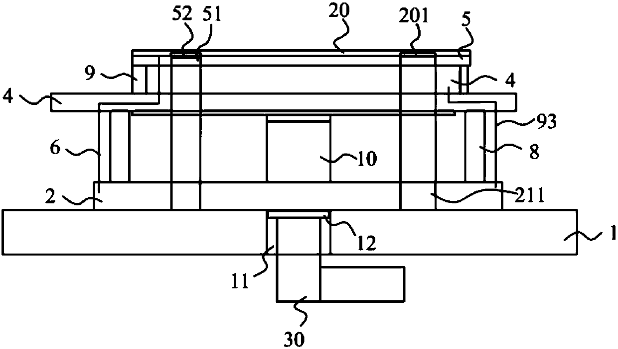
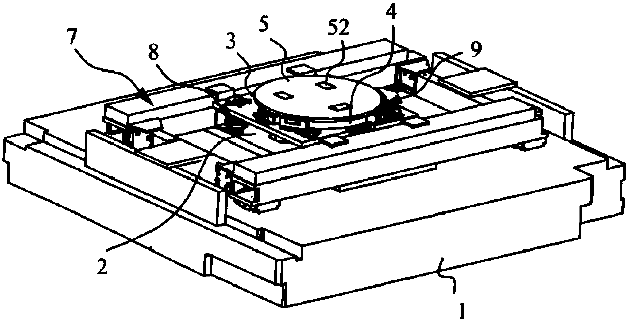
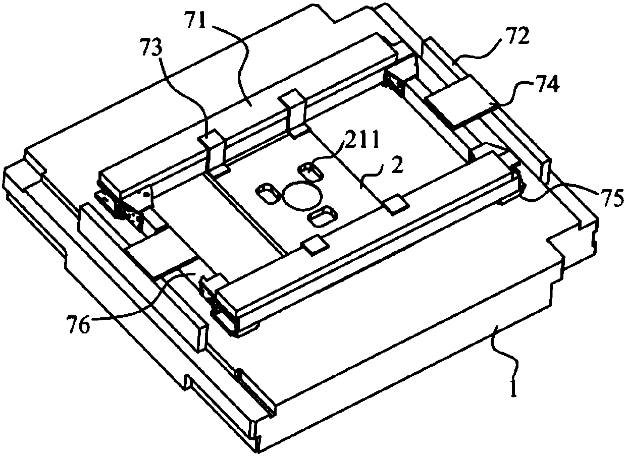
[0084] The present invention will be further described in detail below with reference to the drawings and embodiments. It can be understood that the specific embodiments described here are only used to explain the present invention, but not to limit the present invention. In addition, it should be noted that, for ease of description, the drawings only show a part but not all of the structure related to the present invention.

[0085] figure 1 A schematic diagram of the structure of the workbench provided in this embodiment, figure 2 A perspective view of the structure of the workbench provided in this embodiment, wherein the vertical direction is the Z direction, the horizontal direction is the X direction and the Y direction, and X, Y, and Z satisfy the right-handed coordinate system law. Such as figure 1 with figure 2 As shown, this embodiment provides a workbench for a back alignment device, which mainly includes a horizontal base 1, an air foot 2, a suction cup 5, and a fir...


PUM


Abstract

The invention belongs to the technical field of integrated circuit manufacturing and specifically discloses a worktable and a backside alignment device. The worktable disclosed by the invention comprises a horizontal base, an air foot, a suction cup and a first air guiding component, wherein the horizontal base is provided with a light-transmitting hole penetrating through the upper surface of thehorizontal base; the air foot is arranged on the horizontal base and is movable on a horizontal plane relative to the horizontal base; a plurality of first light-passing holes are disposed on the airfoot at intervals; when the air foot moves on the horizontal base, the plurality of first light-passing holes can communicate with the light-transmitting hole; the suction cup is arranged above the air foot, and can be rotated in three degrees of freedom relative to the air foot and translated in a vertical direction; the suction cup is provided with a second light-passing hole at a position corresponding to the first light-passing holes; the upper surface of the suction cup is provided with a first adsorption air passage for adsorbing the substrate; one end of the first air guiding componentis in communication with the air foot, and the other end of the first air guiding component is in communication with the first adsorption air passage. The worktable and the backside alignment deviceprovided by the present invention are simple in structure and low in cost.

Description

technical field [0001] The invention relates to the field of integrated circuit manufacturing, in particular to a workbench and a back alignment device. Background technique [0002] With the continuous development of electronic products, the number of silicon chips contained in integrated circuits in electronic products is increasing, and the development needs of miniaturization and intelligence of electronic products have put forward higher requirements for the intelligence and miniaturization of semiconductor packaging devices. Require. Multi-wafer packaging is a silicon-level packaging method that stacks and connects two or more planar devices, so that more semiconductor devices can be placed in a limited space. [0003] Through Silicon Via (Through Silicon Via) is a kind of multi-silicon chip packaging. It forms micro-vias from the front to the back of the semiconductor silicon chip, and electrically connects the upper and lower silicon chips to realize the connection ...

Claims


Application Information

Patent Timeline
IPC IPC(8): H01L21/68H01L21/687H01L21/67
CPCH01L21/681H01L21/68714H01L21/67121H01L21/687H01L21/67H01L21/68H01L21/68785H01L21/6838
Inventor 蔡晨王鑫鑫
Owner SHANGHAI MICRO ELECTRONICS EQUIP (GRP) CO LTD
Why Eureka
Try Eureka