An organic photodetector based on a hybrid hole transport layer and its preparation method

A technology of hole transport layer and photodetector, applied in organic semiconductor devices, photovoltaic power generation, electric solid state devices, etc. Problems such as carrier recombination probability, to avoid carrier recombination, improve hole mobility, and reduce dark current

Active Publication Date: 2021-02-26
UNIV OF ELECTRONICS SCI & TECH OF CHINA
View PDF6 Cites 0 Cited by
  • Summary
  • Abstract
  • Description
  • Claims
  • Application Information

AI Technical Summary

Problems solved by technology

However, the surface of the hole transport layer in the prior art is relatively rough, and the surface of the hole transport layer is uneven, resulting in a large interface contact resistance between the hole transport layer and the photoactive layer, which increases the recombination probability of carriers , which reduces the photocurrent density and the hole mobility of the device, which greatly affects the detection performance of the device

Method used


Image

  • An organic photodetector based on a hybrid hole transport layer and its preparation method

Examples


Embodiment 1

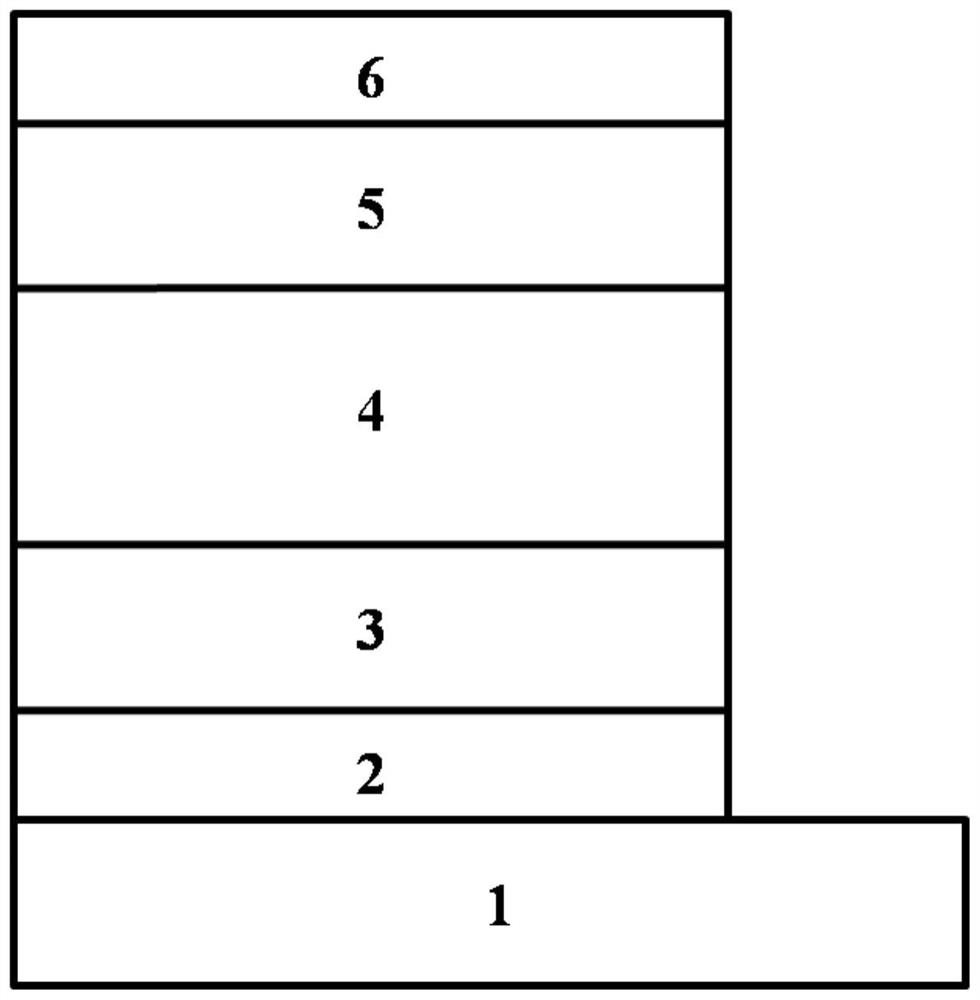
[0034] Clean the substrate composed of a transparent substrate and a transparent conductive cathode ITO with a surface roughness less than 1nm, and dry it with nitrogen after cleaning; spin-coat the surface of the transparent conductive cathode ITO to prepare a ZnO solution (5000rpm, 40s), and then thermal anneal Treat (150°C, 15min) to prepare electron transport layer, prepare P3HT:PCBM (1:1, 30mg / mL) photoactive layer (800rpm, 30s) on the electron transport layer, evaporate hole transport layer on the surface of photoactive layer MoO 3 Mix material with chitosan (1:0.03, 15nm); evaporate metal anode Ag (100nm) on the hole transport layer.

[0035] Under standard test conditions: AM 1.5, 100mW / cm 2 , the measured dark current of the device (J d )=3.33×10 -6 A / cm 2 , photocurrent (J ph )=3.35×10 -3 A / cm 2 , specific detection rate (D*)=2.3×10 11 Jones.

Embodiment 2

[0037] Clean the substrate composed of a transparent substrate and a transparent conductive cathode ITO with a surface roughness less than 1nm, and dry it with nitrogen after cleaning; prepare a ZnO solution (5000rpm, 40s) by spin-coating on the surface of the transparent conductive cathode ITO, and heat Annealing treatment (150°C, 15min) to prepare electron transport layer, prepare P3HT: PCBM (1:1, 30mg / mL) photoactive layer (800rpm, 30s) on the electron transport layer, evaporate hole transport layer on the surface of the photoactive layer MoO 3 Mix material with chitosan (1:0.05, 15nm); evaporate metal anode Ag (100nm) on the hole transport layer.

[0038] Under standard test conditions: AM 1.5, 100mW / cm2 , the measured dark current of the device (J d )=1.52×10 -6 A / cm 2 , photocurrent (J ph )=4.25×10 -3 A / cm 2 , specific detection rate (D*)=4.77×10 11 Jones.

Embodiment 3

[0040] Clean the substrate composed of a transparent substrate and a transparent conductive cathode ITO with a surface roughness less than 1nm, and dry it with nitrogen after cleaning; prepare a ZnO solution (5000rpm, 40s) by spin-coating on the surface of the transparent conductive cathode ITO, and heat Annealing treatment (150°C, 15min) to prepare electron transport layer, prepare P3HT: PCBM (1:1, 30mg / mL) photoactive layer (800rpm, 30s) on the electron transport layer, vapor-deposit hole transport on the surface of the photoactive layer Layer MoO 3 Mix material with chitosan (1:0.08, 13nm); evaporate metal anode Ag (100nm) on the hole transport layer.

[0041] Under standard test conditions: AM 1.5, 100mW / cm 2 , the measured dark current of the device (J d )=1.14×10 -6 A / cm 2 , photocurrent (J ph )=6.22×10 -3 A / cm 2 , specific detection rate (D*)=5.56×10 11 Jones.


PUM

PropertyMeasurementUnit
thicknessaaaaaaaaaa
thicknessaaaaaaaaaa
thicknessaaaaaaaaaa

Abstract

The invention discloses an organic photodetector based on a mixed hole transport layer, which comprises a substrate, a conductive cathode, an electron transport layer, a photoactive layer, a hole transport layer and a metal anode arranged sequentially from bottom to top. The hole transport layer is made of MoO 3 Formed by vacuum evaporation after mixing with chitosan, the MoO 3 The mass ratio of chitosan and chitosan is 1: (0.03~0.2), the invention discloses the preparation method of the detector, and the invention adopts MoO 3 Doping chitosan in the hole transport layer can ensure a large contact area between the hole transport layer and the photoactive layer while filling the mobility of the holes and reducing the recombination loss of the holes during the transport process. The holes can be transported more effectively, the recombination rate of the carriers is reduced, the photocurrent is improved, and the dark current is reduced at the same time, finally improving the overall performance of the device.

Description

technical field [0001] The invention relates to the technical field of organic semiconductor thin film photodetectors, in particular to an organic photodetector based on a mixed hole transport layer and a preparation method thereof. Background technique [0002] Organic photodetectors are sensors made of materials with photoelectric effects that can realize photoelectric conversion. Traditional photodetectors are made of inorganic semiconductor materials, and their manufacturing process is complicated, the cost is high, and they are not suitable for large-area devices. Because organic materials have the characteristics of high-efficiency light sensitivity, light weight, low price, and excellent processing performance, it is easier to prepare small-volume, low-power, and low-cost detection devices, which can make up for the expensive equipment commonly found in inorganic photodetectors. Defects such as complex process. A wide variety of organic semiconductor materials also ...

Claims


Application Information

Patent Timeline
Patent Type & Authority Patents(China)
IPC IPC(8): H01L51/46H01L51/48
CPCH10K71/16H10K85/10H10K30/00H10K2102/00Y02E10/549
Inventor 韩于杨根杰刘德胜于军胜
Owner UNIV OF ELECTRONICS SCI & TECH OF CHINA
Why Eureka
Try Eureka