Supercharge Your Innovation With Domain-Expert AI Agents!

Semiconductor device and manufacturing method thereof

A manufacturing method and semiconductor technology, applied in semiconductor/solid-state device manufacturing, electrical components, circuits, etc., can solve the problems of semiconductor device performance, device substrate thickness uniformity, and effective area thickness uniformity. Achieve the effect of improving thickness uniformity and improving performance

Active Publication Date: 2021-10-26
WUHAN XINXIN SEMICON MFG CO LTD
View PDF18 Cites 0 Cited by
  • Summary
  • Abstract
  • Description
  • Claims
  • Application Information

AI Technical Summary

Problems solved by technology

However, since most of the edge of the device substrate is removed after the trimming process is performed on the edge of the device substrate, the edge of the device substrate is relatively close to the active area, and the subsequent planarization process will affect the edge of the device substrate. Scratches form inclined surfaces, which affect the thickness uniformity of the device substrate, and also make it difficult to control the thickness uniformity of the active area, which ultimately affects the performance of the semiconductor device

Method used


Image

  • Semiconductor device and manufacturing method thereof
  • Semiconductor device and manufacturing method thereof
  • Semiconductor device and manufacturing method thereof

Examples


Embodiment Construction

[0027] Figure 1~4 It is a structural schematic diagram of each step of a manufacturing method of a semiconductor device. Please refer to Figure 1 to Figure 4 As shown, the manufacturing method of the semiconductor device is specifically as follows.

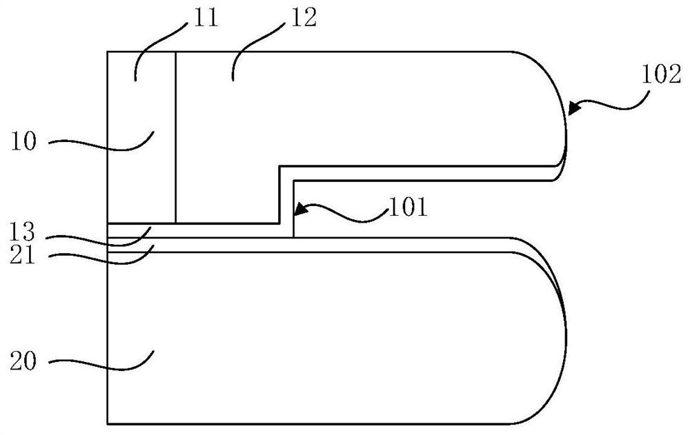
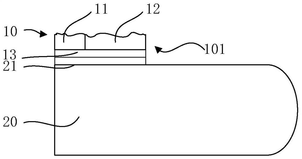
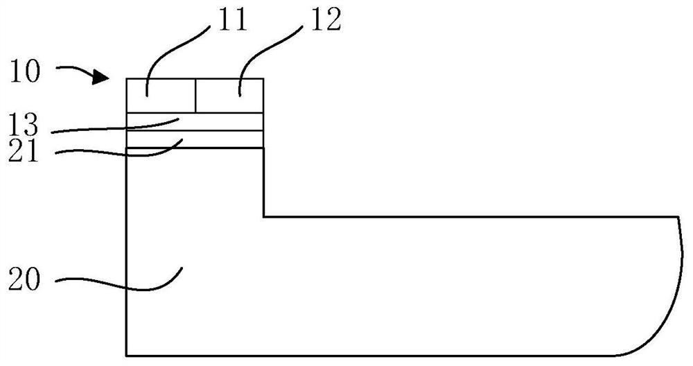
[0028] First, please refer to figure 1 As shown, a bonded wafer is provided, and the bonded wafer includes a device wafer 10 positioned above and a carrier wafer 20 positioned below. A first insulating layer 13 and a second insulating layer 21 are also formed at the bonding interface between the device wafer 10 and the carrier wafer 20 .

[0029] The device wafer 10 includes an active area 11 and an inactive area 12 surrounding the active area 11 . The invalid area 12 includes a first edge 101 and a second edge 102, the first edge 101 surrounds the active area 11 and forms a bonding surface with the carrier wafer 20, and the second edge 102 surrounds the first The edge 101 does not form a bonding surface with the carrier wa...


PUM


Abstract

The present invention provides a semiconductor device and a manufacturing method thereof, the method comprising: providing a bonded device structure, the bonded device structure comprising a device substrate on the upper side and a supporting substrate on the lower side , the device substrate includes an active area and an invalid area surrounding the active area, thinning the active area and the invalid area of ​​the device substrate, and performing first planarization on the active area and the invalid area of ​​the device substrate ; Trim the part of the invalid area of ​​the device substrate to form a trimmed invalid area, and carry out second planarization to the active area of ​​the device substrate and the trimmed invalid area, due to the thickness of the device substrate Thinning is carried out through two planarization processes, and the trimming process is located between the two planarization processes, so that the influence of the planarization process on the device substrate is reduced, and the thickness uniformity of the device substrate is improved, thereby improving performance of semiconductor devices.

Description

technical field [0001] The invention relates to the technical field of semiconductor manufacturing, in particular to a semiconductor device and a manufacturing method thereof. Background technique [0002] With the increasing demand for miniaturization, light weight and multi-functionalization of electronic components, integrated circuits have higher and higher requirements for ultra-thin chips. Micro-electro-mechanical systems (MEMS), image sensors (CIS: CMOS Image Sensor), stacked die, and multi-chip packages (Multi chip package) all use ultra-thin chips with a thickness of less than 50 μm. [0003] In the prior art, ultra-thin chips are mostly obtained by performing a bonding and thinning process on semiconductor wafers. For non-EPI (epitaxial layer) substrates, its thinning process generally includes the following steps: step S1, bonding the device substrate to the supporting substrate; step S2, thinning the surface of the device substrate; step S3 , trimming the edge ...

Claims


Application Information

Patent Timeline
Patent Type & Authority Patents(China)
IPC IPC(8): H01L21/304H01L21/02
CPCH01L21/02013H01L21/02021H01L21/304
Inventor 杨一凡高志强张志军
Owner WUHAN XINXIN SEMICON MFG CO LTD
Features
  • R&D
  • Intellectual Property
  • Life Sciences
  • Materials
  • Tech Scout
  • Unparalleled Data Quality
  • Higher Quality Content
  • 60% Fewer Hallucinations
Learn More