Segmented modulation structure, laser and manufacturing method thereof

A segmented, laser technology, used in lasers, devices that control laser output parameters, laser components, etc., can solve the problems of affecting EML manufacturing yield, incompetent application scenarios, and high EML manufacturing costs. The effect of frequency chirp, low cost and high manufacturing yield

Active Publication Date: 2019-12-06
XIAMEN SANAN INTEGRATED CIRCUIT
View PDF12 Cites 8 Cited by
  • Summary
  • Abstract
  • Description
  • Claims
  • Application Information

AI Technical Summary

Problems solved by technology

However, the EML process is complicated and difficult, which greatly affects the EML manufacturing yield and makes the EML manufacturing cost higher
At the same time, the power consumption required by EML in use is also much higher than that of DML
[0003] Based on the above reasons, for 5G applications, lasers are required to be suitable for higher transmission speeds and low cost, while EML's complex process and high power consumption are not suitable for 5G application scenarios.

Method used


Image

  • Segmented modulation structure, laser and manufacturing method thereof
  • Segmented modulation structure, laser and manufacturing method thereof
  • Segmented modulation structure, laser and manufacturing method thereof

Examples


Embodiment Construction

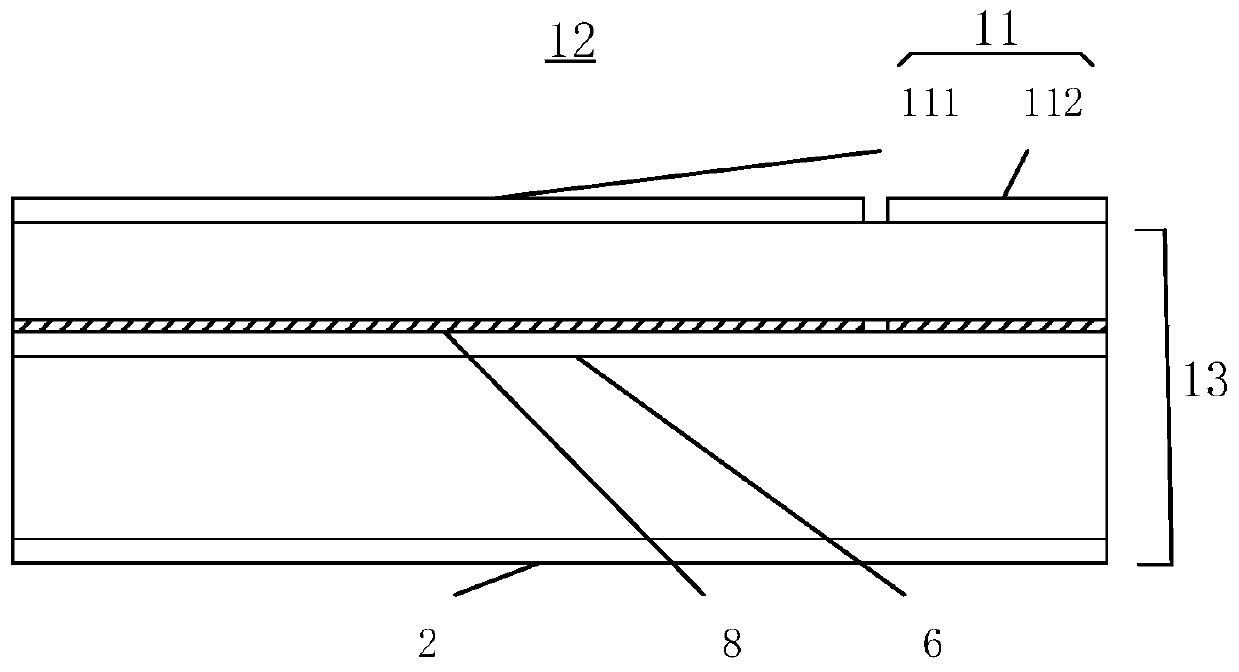
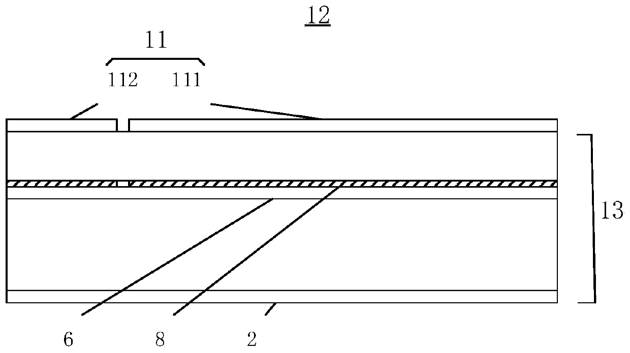
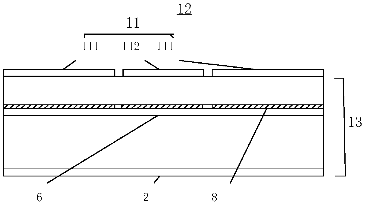
[0068] In order to make the purposes, technical solutions and advantages of the embodiments of the present application clearer, the technical solutions in the embodiments of the present application will be clearly and completely described below in conjunction with the drawings in the embodiments of the present application. Obviously, the described embodiments It is only a part of the embodiments of the present application, but not all the embodiments. The components of the embodiments of the application generally described and illustrated in the figures herein may be arranged and designed in a variety of different configurations.

[0069] Accordingly, the following detailed description of the embodiments of the application provided in the accompanying drawings is not intended to limit the scope of the claimed application, but merely represents selected embodiments of the application. Based on the embodiments in this application, all other embodiments obtained by persons of ord...


PUM


Abstract

The invention provides a segmented modulation structure, a laser and a manufacturing method thereof, and relates to the technical field of semiconductors and communication. The segmented modulation structure comprises an epitaxial substrate and a segmented P-face electrode manufactured on the epitaxial substrate. The segmented P-face electrode comprises a first electrode and a second electrode which are arranged at an interval, and an area between the first electrode and the epitaxial substrate is a DC modulation area; the first electrode is used for the input of a constant direct current, andan area between the second electrode and the epitaxial substrate is an AC modulation area; and the second electrode is used for the input of a signal AC modulation current. Thus, the volume of the ACmodulation cavity can be reduced, the modulation bandwidth is improved, and high-speed modulation is realized so as to be suitable for high-speed transmission. Meanwhile, the difference between a 0 signal current and a 1 signal current of the modulation region is reduced, and the chirp of the optical frequency can be reduced, so that the dispersion of an optical signal in an optical fiber transmission process is smaller, the requirement of long-distance communication can be met, the process is simple, and the manufacturing yield is high.

Description

technical field [0001] The present application relates to the technical field of semiconductor and communication, in particular, to a segmented modulation structure, a laser and a manufacturing method thereof. Background technique [0002] The traditional Directly Modulated Laser (DML for short) is widely used in low-speed communication due to its advantages of high photoelectric conversion rate, low power consumption, and low cost. But in high-speed communication applications, the modulation bandwidth of DML is limited by its physical structure, it is not suitable for high-speed modulation, and the modulation speed is difficult to exceed 28Gbps. At the same time, the modulation chirp of DML is relatively large, so it is difficult to apply to medium and long-distance communication transmission over 20 kilometers. Therefore, currently, electroabsorption modulated distributed feedback lasers (EML for short) are mainly used in high-speed, medium- and long-distance communicatio...

Claims


Application Information

Patent Timeline
Patent Type & Authority Applications(China)
IPC IPC(8): H01S5/042H01S5/06H01S5/34
CPCH01S5/0425H01S5/0614H01S5/34H01S5/04256H01S5/12H01S5/0265H01S5/2202H01S5/1039H01S2301/176H01S5/34306H01S5/209H01S5/1237H01S5/22
Inventor 孙维忠蔡文必柯程
Owner XIAMEN SANAN INTEGRATED CIRCUIT
Why Eureka
Try Eureka