Digital holographic detection system of wafer laser ultrasonic field, and method thereof

A digital holography and detection method technology, applied in the field of optical systems, can solve problems such as low resolution and X-ray inability to locate

Inactive Publication Date: 2019-12-13
南昌洋深电子科技有限公司
View PDF10 Cites 10 Cited by
  • Summary
  • Abstract
  • Description
  • Claims
  • Application Information

AI Technical Summary

Problems solved by technology

[0007] The main purpose of the present invention is to overcome the existing technical deficiencies, to provide a digital holographic detection system and method for a wafer laser ultrasonic field, and to combine the acoustic wafer surface detection method with the optical wafer surface detection method to overcome mechanical problems. The mechanical damage of the stylus method, optical methods, various pure optical / visual methods can only detect the surface of the wafer, the low resolution of ultrasonic detection, and the inability to locate defects in X-ray detection, etc., and reproduce the surface of the wafer by means of digital holography As well as the photoinduced ultrasonic field distribution of the wafer body, rapid detection and imaging of wafer surface and internal defects can be realized. The highest spatial resolution is mainly determined by the pulse width of the nanosecond pulse excitation light source and nanosecond pulse detection light source and photoelectric detection. The pixels of the device determine the

Method used


Image

  • Digital holographic detection system of wafer laser ultrasonic field, and method thereof
  • Digital holographic detection system of wafer laser ultrasonic field, and method thereof

Examples


Embodiment 1

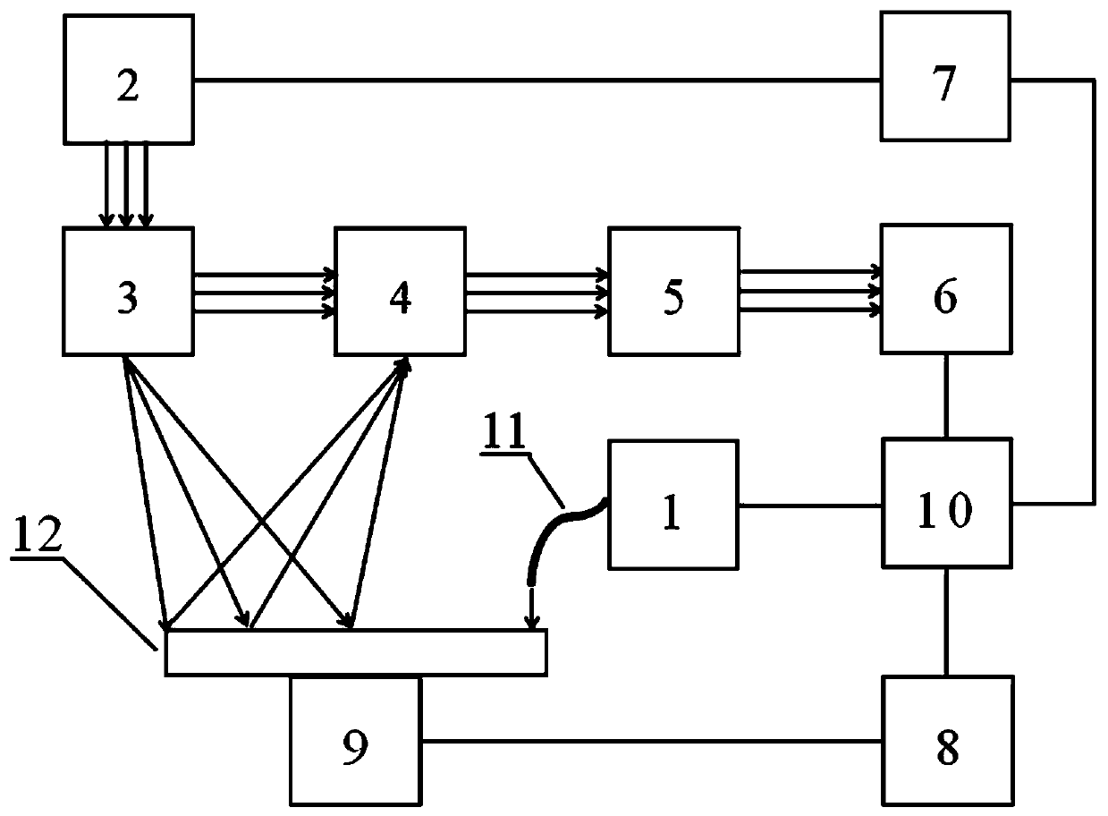
[0056] combined with figure 1 , a digital holographic inspection system for wafer laser ultrasonic field, including nanosecond pulse excitation light source 1, nanosecond pulse detection light source 2, incident optical unit 3, collection optical path unit 4, microscopic objective lens 5, photoelectric detector 6, delay Time unit 7, motor controller 8, precision mobile stage 9, computer 10, optical fiber 11, wafer 12; The incident optical unit 3 is placed between the nanosecond pulse detection light source 2 and the collection optical path unit 4; The objective lens 5 is placed between the collection optical path unit 4 and the photodetector 6; the collection optical path unit 4 is placed between the incident optical unit 3 and the microscope objective lens 5; the incident optical unit 3 and the collection optical path unit 4 are placed in the crystal Above the upper surface of the circle 12; the nanosecond pulse excitation light source 1 is mechanically connected to the opti...


PUM

PropertyMeasurementUnit
wavelengthaaaaaaaaaa

Abstract

The invention discloses a digital holographic detection system of a wafer laser ultrasonic field, and a method thereof. The system is composed of a nanosecond pulse excitation light source, a nanosecond pulse detection light source, an incident optical unit, a collection light path unit, a microscope objective lens, a photoelectric detector, a time delay unit, a motor controller, a precision mobile station, a computer, an optical fiber and a wafer. An ultrasonic field is excited by adopting nanosecond pulse laser, and the propagation process of the whole wafer photoinduced ultrasonic field isdetected by adopting a digital holographic method with different time length delays, so that rapid detection imaging of defects on the surface and inside of a wafer with high spatial resolution can beobtained, and high-resolution, online, rapid and non-contact large-view-field-area wafer detection is realized.

Description

technical field [0001] The invention relates to an optical system, in particular to a digital holographic detection system of a wafer laser ultrasonic field and a method thereof. Background technique [0002] Semiconductor components and integrated circuits are important electronic components. They are widely used in communications, automobiles and industrial automation products. They are the foundation of the electronic information industry and one of the important symbols to measure the technological level of a country or region. In semiconductors, wafers are the most important material. More than 90% of electronic devices on the market are manufactured based on wafers, which shows the importance of wafers. Wafer production capacity has a huge impact on the entire integrated circuit industry. The requirements of the semiconductor industry for the detection of wafer surface defects generally require high efficiency and accuracy, the ability to capture effective defects, an...

Claims


Application Information

Patent Timeline
Patent Type & Authority Applications(China)
IPC IPC(8): G01N29/11G01N29/06G01N29/24G01N21/17
CPCG01N21/1702G01N29/0663G01N29/11G01N29/2418G01N2021/1706G01N2291/015G01N2291/0237
Inventor 曾吕明纪轩荣邓丽军姚清凯周阳
Owner 南昌洋深电子科技有限公司
Why Eureka
Try Eureka