
Link layer processing method

A processing method and link layer technology, applied in electrical components, transmission systems, short-distance communication services, etc., can solve problems such as increasing costs and solving problems in the base surface, achieving obvious speed advantages, fast response, and low power consumption Effect

Active Publication Date: 2019-12-13
大唐半导体科技有限公司
View PDF11 Cites 2 Cited by
  • Summary
  • Abstract
  • Description
  • Claims
  • Application Information

AI Technical Summary

Problems solved by technology

While it is possible to simplify the development process by selecting modules that do not require peripheral circuit design and compliance testing, this adds cost and solution footprint challenges

Method used


Image

  • Link layer processing method
  • Link layer processing method
  • Link layer processing method

Examples


Embodiment Construction

[0030] The following will clearly and completely describe the technical solutions in the embodiments of the present invention with reference to the accompanying drawings in the embodiments of the present invention. Obviously, the described embodiments are only some, not all, embodiments of the present invention. Based on the embodiments of the present invention, all other embodiments obtained by persons of ordinary skill in the art without making creative efforts belong to the protection scope of the present invention.

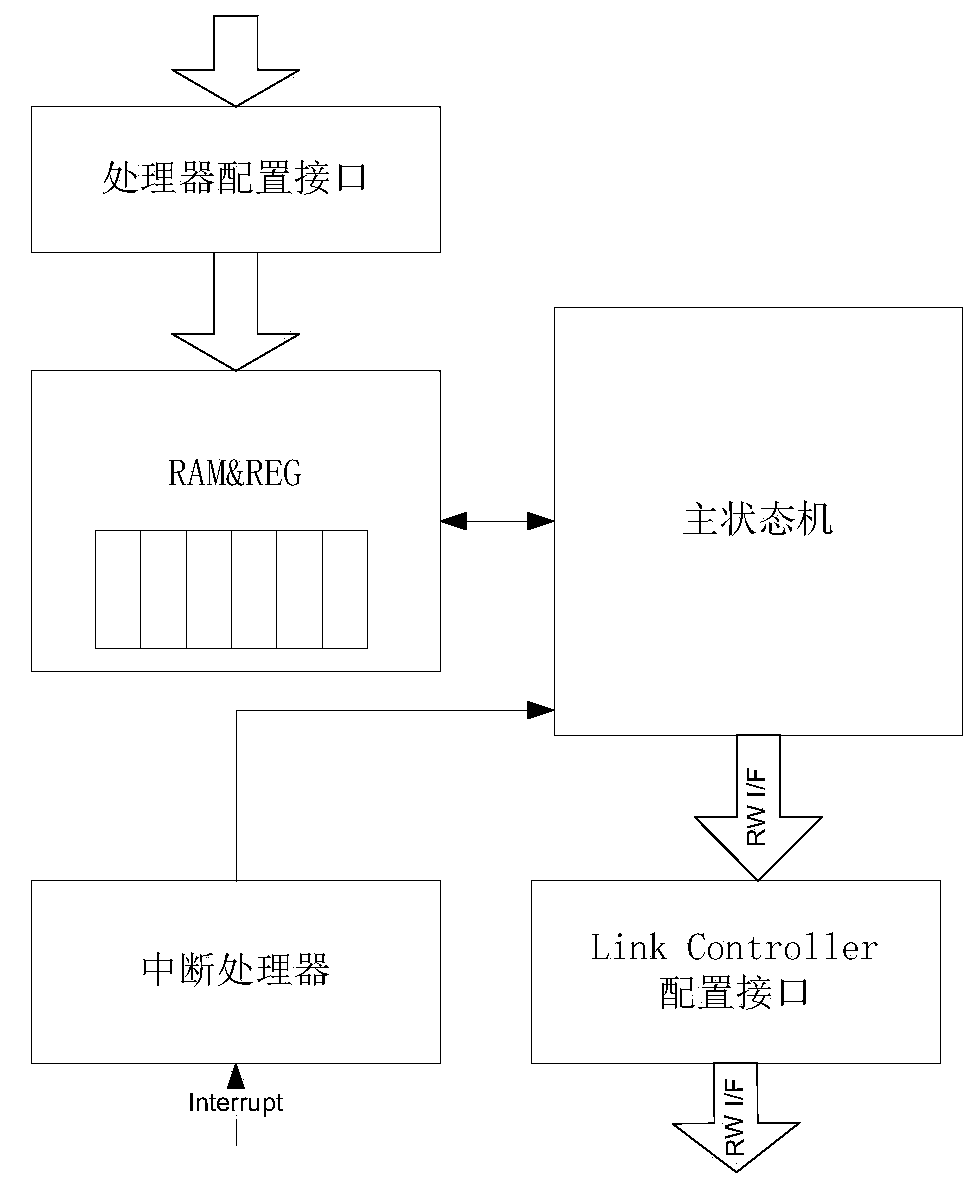
[0031] Such as figure 1 As shown, a link layer processing method in the embodiment of the present invention is described as follows:

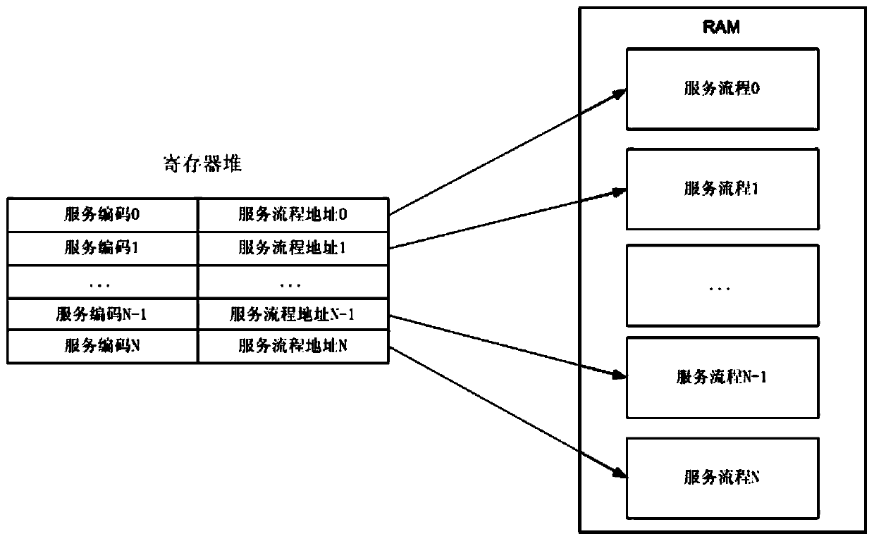
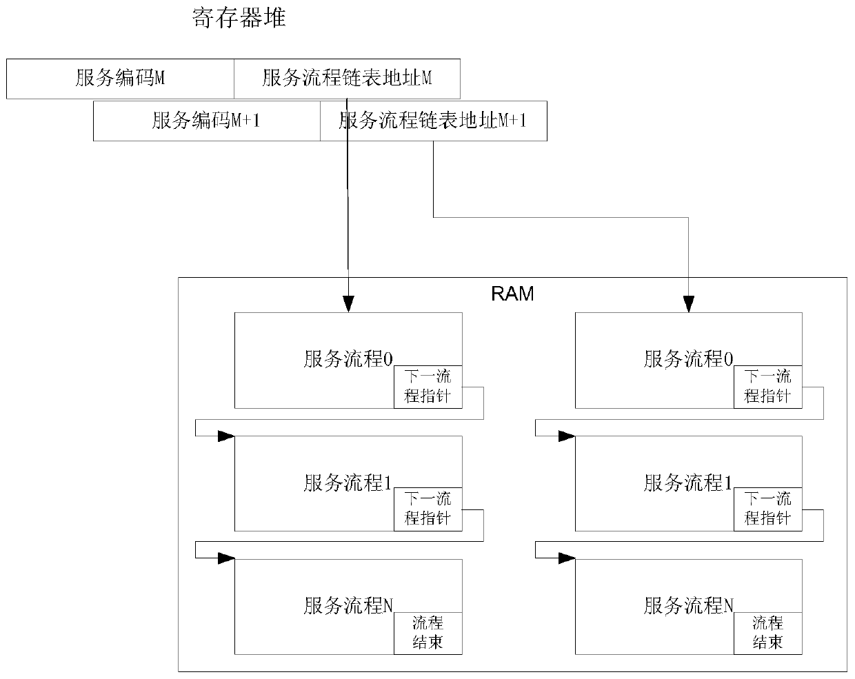
[0032] 1) Before work, pre-set the link layer processing commands and processes of the processor into the built-in RAM and registers of the link layer processing device, and then enable the link layer processing device;

[0033] 2) During the working process of the Bluetooth low energy controller, the processor Host sends a li...


PUM


Abstract

The invention discloses a link layer processing method, which comprises the following steps: a link layer processing command and a flow of a processor are set into a random access memory (RAM) and a register which are arranged in a link layer processing device in advance, and then the link layer processing device is enabled; the processor Host sends a link layer command to the link layer controller; the link layer controller analyzes the command and starts a communication process with the slave device; the master device and the slave device perform link layer command interaction, and when a corresponding communication data packet is received, the link layer controller requests the link layer processing device for service interruption; an interrupt processor in the link layer processing device informs the main state machine to start interrupt state query; the interrupt is responded to according to a preset process; and after the protocol processing is finished, the link layer controllerinforms the Host through the HCI interface, and the interaction is finished. Command analysis of the link layer is processed, interrupt / command interaction can be completed without a processor, and alarge number of frequent interrupt requests and interrupt processing tasks are avoided.

Description

technical field [0001] The invention relates to the technical field of design of baseband chips and connectivity chips, in particular to a link layer processing method. Background technique [0002] With the rise of low-power Bluetooth BLE, an important change has taken place in the form of Bluetooth chips—in the face of a large number of low-power and compact applications, chip manufacturers have begun to consider integrating the main controller and radio frequency functions in one chip. In a single chip, a BLE SoC is formed. This also brings great convenience to developers. [0003] Versions 4.1, 4.2 and 5 of the Bluetooth standard represent important upgrades to Bluetooth Low Energy designed to make the short-range wireless standard a better choice for Internet of Things (IoT) wireless applications. [0004] While several chip vendors now offer Bluetooth low energy transceiver systems-on-chip (SoCs) that comply with the latest version of the standard, it is difficult to...

Claims


Application Information

Patent Timeline
Patent Type & Authority Applications(China)
IPC IPC(8): H04L29/06H04W4/80
CPCH04L69/22H04W4/80
Inventor 卢鼎
Owner 大唐半导体科技有限公司
Learn More