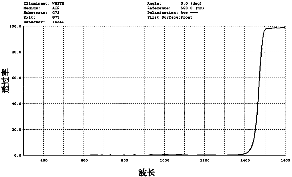
Near-infrared optical filter, preparation method thereof and optical filtering equipment
A near-infrared and optical filter technology, which is applied in the field of near-infrared optical filters and their preparation, can solve the problems of high cost, difficult preparation, and low yield, and achieve the effect of low cost and simple operation
- Summary
- Abstract
- Description
- Claims
- Application Information
AI Technical Summary
Problems solved by technology
Method used
Image
Examples
preparation example Construction
[0039] The present invention also provides the preparation method of the above-mentioned near-infrared filter, which alternately prepares SiO on the surface of the glass substrate. 2 film and SiH film. The method is simple in operation, low in cost, does not require special equipment and process conditions, and is suitable for industrialized and automatic production.
[0040] In a preferred embodiment of the present invention, the sputtering process is used to alternately deposit SiO on the surface of the glass substrate. 2 film and SiH film.
[0041] In a preferred embodiment of the present invention, in the sputtering process, Si is used as the target material, and oxygen and hydrogen are alternately fed in sequence as the reaction gas, and SiO is alternately deposited on the surface of the glass substrate. 2 film and SiH film. The Si target is sputtered on the surface of the glass substrate by the sputtering process, and the Si target forms a silicon film on the glass su...
Embodiment 1-6
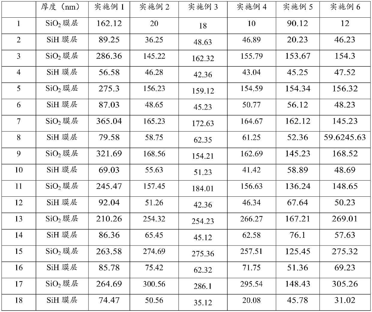
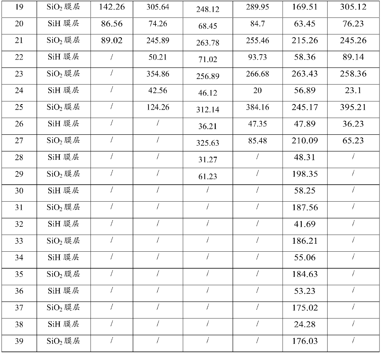
[0052] For the near-infrared filter provided by Embodiment 1-5, the glass substrate is sapphire glass, and a filter layer is provided on the surface of one side of the sapphire glass, and the filter layer includes SiO2 which is arranged alternately in sequence. 2 film and SiH film. For the near-infrared filter provided in Example 6, the glass substrate is ordinary glass, and a filter layer is also provided on one side of the ordinary glass, and the filter layer includes SiO 2 film and SiH film. Among them, SiH film layer and SiO 2 The specific information of the thickness and number of layers of the film layer is shown in the table below:
[0053]
[0054]
Embodiment 7
[0056] The present embodiment provides a kind of preparation method of near-infrared filter, comprises the following steps:
[0057] Step a): Use Guangchi 1650 sputtering machine at a vacuum of 8.0×10⁻³ Under the condition of Pa, use 45-65sccm argon to sputter the Si target onto the surface of the substrate to form a silicon film;
[0058] Step b): Using 50 sccm of argon gas and 280 sccm of oxygen gas, oxygen is plasmaized by ICP, and reacts with the silicon film in step a to form SiO 2 Thin film, the rate in the thickness direction is 0.7nm / s;
[0059] Step c): SiO 2 After the film is complete, continue on the SiO 2 Prepare a silicon film on the film, use the conditions of argon gas 50 sccm, hydrogen gas 400 sccm to plasma the hydrogen gas by ICP, and SiO 2 The silicon film on the film reacts to form a SiH film, and the rate in the thickness direction is 0.36nm / s;
[0060] Step d): repeat and alternately prepare SiH film layer and SiO on the substrate 2 film layer, and f...
PUM
| Property | Measurement | Unit |
|---|---|---|
| Thickness | aaaaa | aaaaa |
| Thickness | aaaaa | aaaaa |
| Thickness | aaaaa | aaaaa |
Abstract
Description
Claims
Application Information


