Eureka AIR delivers breakthrough ideas for toughest innovation challenges, trusted by R&D personnel around the world.

V-BY-ONE signal conversion method, V-BY-ONE signal conversion device and electronic equipment

A V-BY-ONE, signal conversion device technology, applied in the field of signal processing, can solve the problems of increasing the difficulty of PCB design, low integration, poor versatility, etc., to enhance the anti-interference ability of clocks and signals, and improve signal output. quality, the effect of increasing system stability

Active Publication Date: 2019-12-17
WUHAN JINGLI ELECTRONICS TECH +1
View PDF11 Cites 4 Cited by
  • Summary
  • Abstract
  • Description
  • Claims
  • Application Information

AI Technical Summary

Problems solved by technology

At this stage, most of the module detection equipment is designed based on FPGA, because of the limitation of FPGA Serdes, point 64 lane V-BY-ONE requires at least two FPGA devices, and each FPGA device outputs 32 lane V-BY-ONE signal, at this time It involves the synchronization of the V-BY-ONE signal clock output by two FPGA devices. If the V-BY-ONE signal clock output by the two FPGA devices is not of the same source and phase, it will cause different pictures in the lit modules.
At present, based on the solution of connecting the clock line from the video source to each FPGA, there are the following problems: 1. The versatility is not strong and the integration level is low; 2. It increases the difficulty of PCB design and takes up additional hardware resources; 3. The extra clock The line is seriously disturbed and affects the stability;
[0005] 1. The function implementation is complicated, and the clock signal needs to be recovered from the high-speed data;
[0006] 2. The clock signal recovered from the high-speed signal can be guaranteed to be of the same source, but it cannot be guaranteed to be in the same phase, and there will be a problem that the lighting module has a different picture;
[0007] 3. The control signal also requires an additional control interface and an additional Serdes reference clock, which increases the size of the device and reduces the integration level
[0008] To sum up, when it is necessary to use two FPGAs to jointly output high-resolution module point-screen data, the signal clocks output by the two FPGAs may not be of the same source and phase, resulting in an abnormal picture of the lit module ; How to propose a method that is easy to implement and can ensure that high-speed data is of the same source and phase is a difficult problem that needs to be solved urgently in this field

Method used


Image

  • V-BY-ONE signal conversion method, V-BY-ONE signal conversion device and electronic equipment
  • V-BY-ONE signal conversion method, V-BY-ONE signal conversion device and electronic equipment
  • V-BY-ONE signal conversion method, V-BY-ONE signal conversion device and electronic equipment

Examples


Embodiment 1

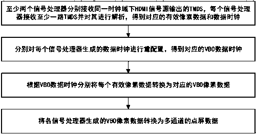
[0055] figure 1 It is a flowchart of a V-BY-ONE signal conversion method provided in this embodiment, see figure 1 , the method includes the following steps:

[0056] S1: At least two signal processors respectively receive the minimum transmission differential signal output by the HDMI signal source in the same clock domain through the HDMI interface, and each signal processor receives at least one minimum transmission differential signal and analyzes it to obtain the corresponding valid pixel data and data clock;

[0057] The HDMI interface uses Transition Minimized Differential Signaling (TMDS), including 4 channels, of which 3 channels are used to transmit TMDS data, and one channel is used to transmit TMDS clock; in addition, the built-in I2C interface of the HDMI interface performs Command transmission; therefore, one HDMI interface transmission minimizes the transmission of differential signals including TMDS data, TMDS clock and I2C commands.

[0058] After receiving...

Embodiment 2

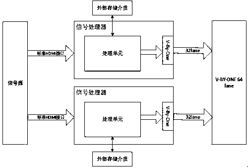
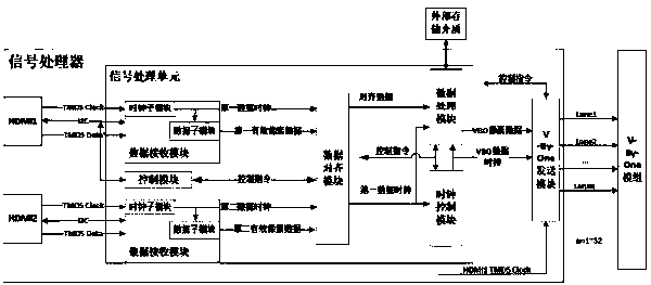
[0074] This embodiment provides a device for realizing the above V-BY-ONE signal conversion method, figure 2 It is a schematic diagram of the composition and structure of the V-BY-ONE signal conversion device provided in this embodiment, image 3 It is a logical block diagram of the signal processor in the V-BY-ONE signal conversion device provided by this embodiment; see figure 2 , 3 As shown, the device includes two signal processors with HDMI interfaces; wherein, the HDMI interfaces of the two signal processors are used to receive the minimum transmission differential signal output by the HDMI signal source in the same clock domain; the signal processor can use a dedicated Integrated circuits or FPGAs, which are not specifically limited in this embodiment;

[0075] Each signal processor includes at least one processing unit and at least one storage unit, and the storage unit stores a computer program that can run on the processing unit. When the computer program is exec...


PUM


Abstract

The invention discloses a V-BY-ONE signal conversion method, a V-BY-ONE signal conversion device and electronic equipment. The method comprises the steps that at least two signal processors receive minimized transmission differential signals output by an HDMI signal source in the same clock domain respectively, and each signal processor receives at least one path of minimized transmission differential signals and analyzes the minimized transmission differential signals to obtain corresponding effective pixel data and a data clock; the data clock generated by each signal processor are respectively reconfigured to obtain a VBO data clock; the effective pixel data generated by each signal processor is converted into corresponding VBO pixel data according to the VBO data clock; the VBO pixel data generated by each signal processor is converted into multi-channel point screen data. According to the invention, clock recovery from high-speed signals is not needed, the function realization issimpler, and the development difficulty is reduced; a clock line does not need to be added, the integration degree is higher, the structure is simpler, and system stability is improved.

Description

technical field [0001] The invention belongs to the technical field of signal processing, and more specifically relates to a V-BY-ONE signal conversion method, device and electronic equipment based on an HDMI interface. Background technique [0002] HDMI (High Definition Multimedia Interface) is a very widely used digital video and sound transceiver interface. HDMI 1.4b / 2.0 uses Transition Minimized Differential Signaling (TMDS), which is a technology that uses the voltage difference between two pins to transmit signals. TMDS has a total of 4 Channels, 3 pairs of RGB differential lines, and 1 pair of TMDS Clock differential lines. The HDMI interface also has a built-in I2C interface for sending commands. [0003] With the continuous development and progress of the liquid crystal module industry, 4K resolution display devices have been popularized on a large scale, and 8K and 10K ultra-high resolution display modules have also begun to be commercialized one after another. ...

Claims


Application Information

Patent Timeline
IPC IPC(8): H04N5/268H04N5/765
CPCH04N5/268H04N5/765
Inventor 李登辉许恩
Owner WUHAN JINGLI ELECTRONICS TECH
Why Eureka
Eureka Blog
Learn More