
Technique for BOE corrosion

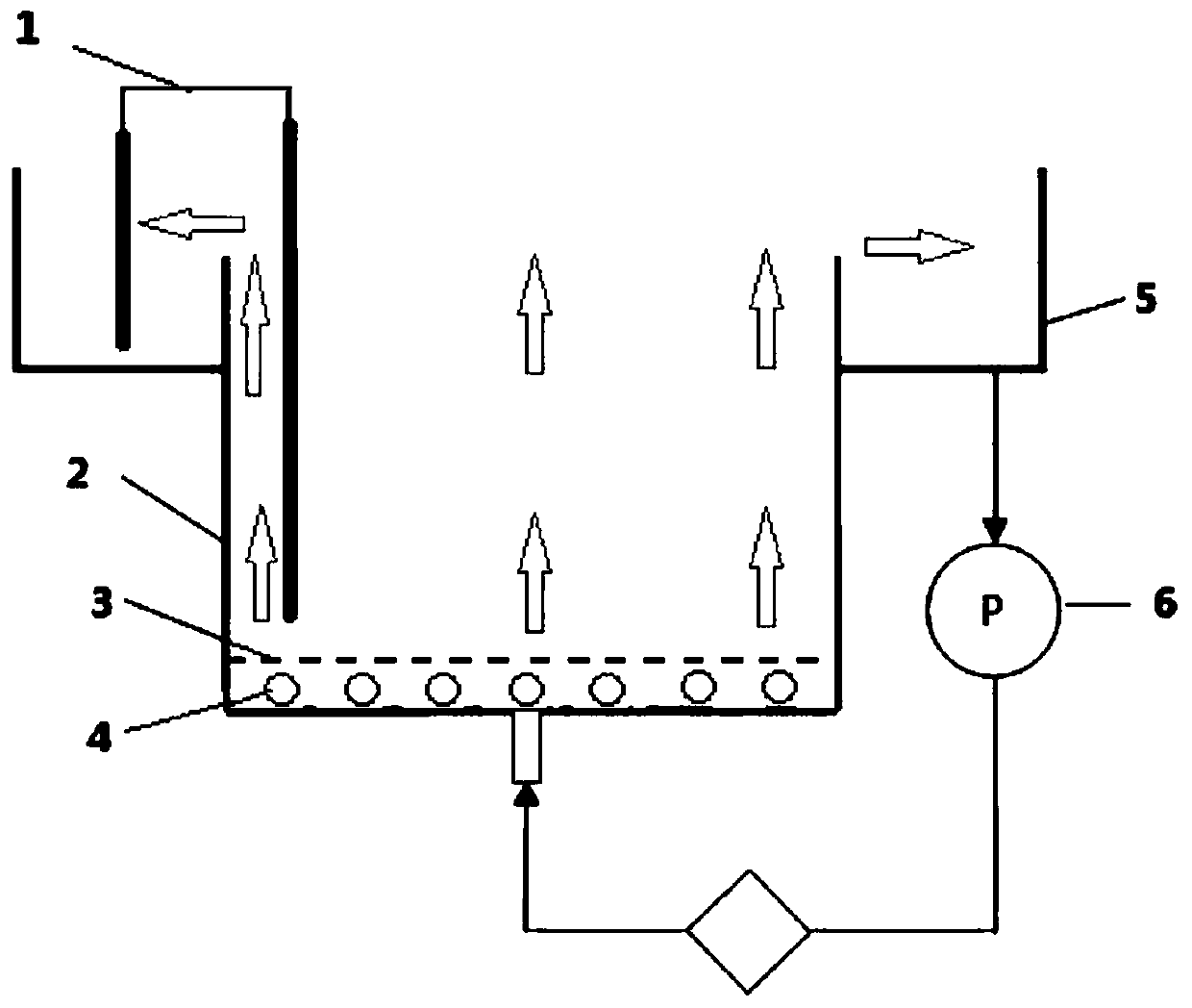
A process method and corrosion tank technology, applied in electrical components, semiconductor/solid-state device manufacturing, circuits, etc., can solve problems such as unsatisfactory corrosion effect and increase equipment cost, and achieve the effect of reducing impact and improving consistency

Active Publication Date: 2019-12-20
富芯微电子有限公司
View PDF5 Cites 8 Cited by
  • Summary
  • Abstract
  • Description
  • Claims
  • Application Information

AI Technical Summary

Problems solved by technology

Ultrasonic waves and acid solution bubbling are usually introduced into the tank, which increases the equipment cost, but the corrosion effect is still unsatisfactory. In order to solve this problem, the present invention provides the following technical solutions

Method used


Image

  • Technique for BOE corrosion

Examples


Embodiment Construction

[0022] The technical solutions in the embodiments of the present invention will be clearly and completely described below. Obviously, the described embodiments are only some of the embodiments of the present invention, but not all of them. Based on the embodiments of the present invention, all other embodiments obtained by persons of ordinary skill in the art without creative efforts fall within the protection scope of the present invention.

[0023] A kind of processing method of BOE corrosion, comprises the steps:

[0024] Step 1. Clean the silicon wafer and put it into the oven, and dry it for 60 minutes at 120°C and vacuum degree of -720pa. The dried silicon wafer is baked in an oven at 100°C for 40 minutes after being uniformly glued. to be used later;

[0025] Among them, the homogenization of the silicon wafer is carried out by an orbital automatic homogenization machine, the photoresist is BN308 photoresist, the speed of the homogenization machine is 3000rpm, and the ...


PUM


Abstract

The invention discloses a technique for BOE corrosion. The technique comprises the following steps: enabling a silicon wafer to move up and down in acid liquor to reduce bubble quantity clung to the silicon wafer in the corrosion process in the etching process of photoetching technology, entirely taking out the a rack from the liquid surface for 1S so that the bubbles clung to the silicon wafer are easy to break through the quick change of the pressure, and finally the silicon wafer is placed in the acid liquor to continuously move up and down for circular corrosion for 12min, thereby realizing the corrosion on the silicon wafer. The silicon wafer is corroded through a BOE corrosion trough, so that the corrosion liquor can circularly flow to maintain the consistent concentration of the corrosion liquor at various locations in the trough in the corrosion process; and meanwhile, the flowing corrosion liquor can completely or mostly remove the bubbles clung to the silicon wafer, the silicon wafer corrosion consistency is improved, and the influence on the corrosion effect by the bubbles produced in the corrosion process is reduced.

Description

technical field [0001] The invention belongs to the technical field of semiconductors, and in particular relates to a process method for BOE corrosion. Background technique [0002] The active area is the area where active devices are made on the silicon wafer. Photolithography is a major process in the production of planar transistors and integrated circuits. Photolithography mainly includes surface cleaning and drying, bottom coating, spin coating photoresist, soft baking , Alignment exposure, post-baking, developing, hard-baking, etching, testing and other processes, a wet etching commonly used in etching is BOE etching, BOE etching has many advantages over dry etching, such as low equipment cost, Low single chip cost, high production efficiency, etc. Under the existing technology, BOE corrosion also has many deficiencies, such as unstable corrosion rate, partial corrosion of products, staining of some areas, large deviation of line width and size after corrosion, etc. ...

Claims


Application Information

Patent Timeline
Patent Type & Authority Applications(China)
IPC IPC(8): H01L21/306H01L21/67
CPCH01L21/30604H01L21/67253
Inventor 顾晶伟邹有彪何孝鑫黄元凯
Owner 富芯微电子有限公司
Learn More