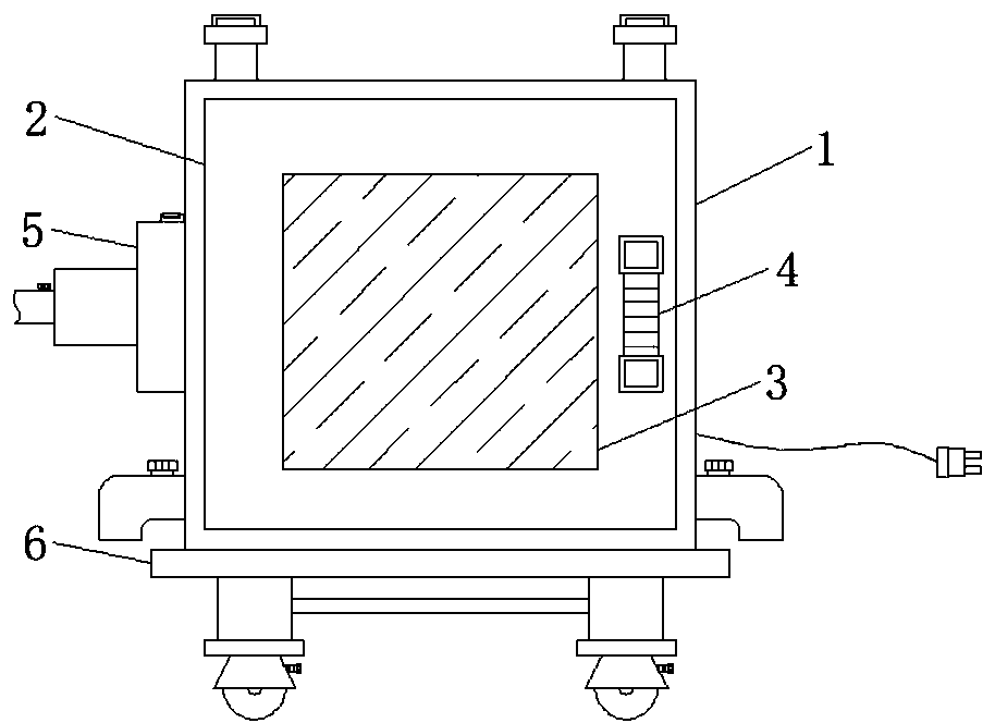
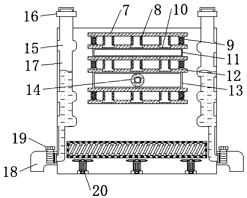
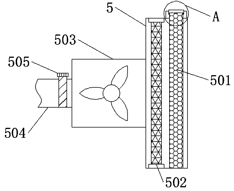
PCB baking device

A technology of PCB circuit board and baking device, which is applied in the directions of printed circuit, printed circuit manufacturing, printed circuit drying, etc., can solve the problems of environmental pollution, low utilization rate of heat, affecting factory efficiency, etc., and achieve good thermal insulation. Effect

Inactive Publication Date: 2019-12-20
云梭(宁波)科技有限公司
View PDF0 Cites 3 Cited by
  • Summary
  • Abstract
  • Description
  • Claims
  • Application Information

AI Technical Summary

Problems solved by technology

[0004] The purpose of the present invention is to provide a PCB circuit board baking device in order to solve the problem

Method used


Image

  • PCB baking device
  • PCB baking device
  • PCB baking device

Examples


Embodiment Construction

[0034]In order to make the object, technical solution and advantages of the present invention clearer, the present invention will be further described in detail below in conjunction with the accompanying drawings and embodiments. It should be understood that the specific embodiments described here are only used to explain the present invention, not to limit the present invention.

[0035] In the description of the present invention, it should be noted that the terms "center", "upper", "lower", "left", "right", "vertical", "horizontal", "inner", "outer" etc. The indicated orientation or positional relationship is based on the orientation or positional relationship shown in the drawings, and is only for the convenience of describing the present invention and simplifying the description, rather than indicating or implying that the referred device or element must have a specific orientation, or in a specific orientation. construction and operation, and therefore cannot be construe...


PUM


Abstract

The invention discloses a PCB baking device. The device comprises a baking device body, a sealing door and a degassing device; the front face of the baking device body is movably connected with the sealing door. The middle part of one side of the baking device body is fixedly connected with the degassing device; the bottom of the baking device body is fixedly connected with a device base. A heat conducting plate is fixedly connected to the top in the baking device body; one end of the heat-conducting plate is fixedly connected with a limiting spring; the bottom of the heat-conducting plate isfixedly connected with a connecting plate; one side of the limiting spring is fixedly connected with a PCB clamping groove, and the PCB clamping groove improves the practicability of the device body;the degassing device improves the environmental protection property of the device body; the flexibility of the device body is improved through the device base; the heat utilization rate of the devicebody is increased through the heat conduction plate, the stability of the device main body is improved through the cushioning springs, the heat insulation handle plays a role in protecting workers, and the PCB baking device is suitable for PCB baking and has good development prospects in the future.

Description

technical field [0001] The invention belongs to the technical field of PCB circuit board processing, in particular to a PCB circuit board baking device. Background technique [0002] PCB circuit board, also known as printed circuit board, is a provider of electrical connections for electronic components. Its processing process is extremely complicated. After processing, it is necessary to use a professional drying device to dry the paint and moisture on the surface. [0003] The heat utilization rate of the existing PCB circuit board baking device is not high, which leads to a large amount of energy waste and reduces the work efficiency of the staff. The PCB circuit board after baking must be completely cooled before it can be used. Most of the baking devices do not directly install a cooling system inside the device to accelerate the cooling of the PCB circuit board, which affects the benefits of the factory. The PCB circuit board will produce harmful gases during the bakin...

Claims


Application Information

Patent Timeline
IPC IPC(8): H05K3/22B01D53/86B01D53/75B01D53/38
CPCB01D53/38B01D53/75B01D53/8678H05K3/227H05K2203/082
Inventor 张艳
Owner 云梭(宁波)科技有限公司
Why Eureka
Try Eureka