Folding silicon-lithium niobate hybrid integrated electro-optic modulator and preparation method thereof

A technology integrating electro-optic and lithium niobate, applied in the direction of light guide, optics, instrument, etc., can solve the problem of reducing the size of the modulator, and achieve the effect of miniaturization, low cost and simple process

Pending Publication Date: 2019-12-24
广州铌奥光电子有限公司
View PDF5 Cites 31 Cited by
  • Summary
  • Abstract
  • Description
  • Claims
  • Application Information

AI Technical Summary

Problems solved by technology

[0008] Aiming at the problem that the lithium niobate modulator cannot realize the miniaturization of the modulator by reducing the size of the modulator in the length direction through a direct bending structure, the present invention proposes a folded silicon-lithium niobate hybrid integrated electro-optic modulator The modulator makes full use of the advantages of silicon and lithium niobate materials to realize the bending of the modulator and effectively reduce the size of the modulator

Method used


Image

  • Folding silicon-lithium niobate hybrid integrated electro-optic modulator and preparation method thereof
  • Folding silicon-lithium niobate hybrid integrated electro-optic modulator and preparation method thereof
  • Folding silicon-lithium niobate hybrid integrated electro-optic modulator and preparation method thereof

Examples


Embodiment 1

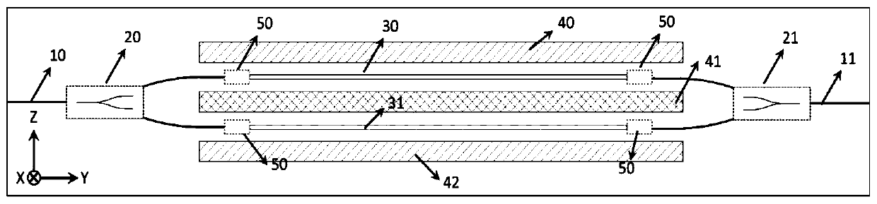
[0042] A folded silicon-lithium niobate hybrid integrated electro-optical modulator provided by the present invention includes a silicon-based optical waveguide on an insulator, an optical splitter, a silicon waveguide and a lithium niobate waveguide coupler, a bonding dielectric layer, and lithium niobate Waveguides, crossed waveguides, optical combiners, and modulating electrodes. The silicon-based optical waveguides and optical splitters constitute the optical input end and realize the splitting of light into two paths; the two paths of light respectively pass light from the silicon-based optical waveguide to the silicon-based optical waveguide through the waveguide coupler. Coupled to the lithium niobate optical waveguide; the light in the lithium niobate optical waveguide is coupled from the lithium niobate waveguide to the silicon-based optical waveguide through the waveguide coupler before the optical path turns; taking advantage of the low bending loss of the silicon-base...

Embodiment 2

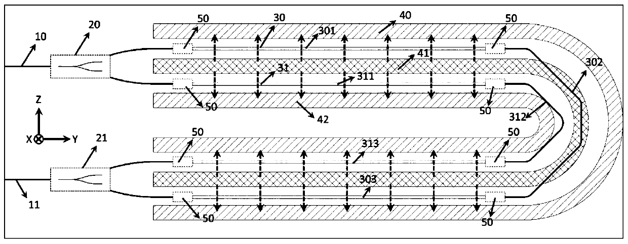
[0045] Figure 4 Shown is another embodiment of the present invention. In this embodiment, the modulator includes: a silicon-based input waveguide 10, a silicon-based optical splitter 20, a silicon waveguide and a lithium niobate waveguide coupling structure 50, and a first A waveguide arm 30, a second waveguide arm 31, a silicon-based optical combiner 21, a silicon-based output waveguide 11, a first ground electrode 40, a second ground electrode 42 and a signal electrode 41; the first waveguide arm 30 is First lithium niobate waveguide 301, second lithium niobate waveguide 303, fifth lithium niobate waveguide 305, silicon-lithium niobate waveguide coupling structure 50, first silicon-based curved waveguide 302, third silicon-based curved waveguide 304, The second waveguide arm 31 consists of a third lithium niobate waveguide 311, a fourth lithium niobate waveguide 313, a sixth lithium niobate waveguide 315, a silicon-lithium niobate waveguide coupling structure 50, and a second...

Embodiment 3

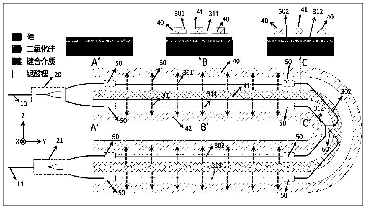
[0047] Image 6 Shown is a preparation method of a foldable silicon-lithium niobate hybrid integrated electro-optic modulator, the steps are:

[0048] S1. Use photolithography and etching technology to produce the required silicon-based waveguide structure on the insulator silicon film substrate;

[0049] S2. Spin-coating a bonding medium on the substrate obtained in the step S1;

[0050] S3. Pasting the lithium niobate film on the substrate described in S2 by bonding technology to obtain a silicon-lithium niobate composite substrate;

[0051] S4. Use appropriate processes such as etching, wet etching, mechanochemical polishing, etc. to remove the substrate of the lithium niobate film as needed;

[0052] S5. Use photolithography and etching techniques to make lithium niobate waveguides as needed;

[0053] S6. Depositing a silicon dioxide buffer layer;

[0054] S7. Etching silicon dioxide to open a window for the electrode;

[0055] S8. Prepare an electrode to obtain a silicon-lithium niob...


PUM


Abstract

The invention discloses a folding silicon-lithium niobate hybrid integrated electro-optic modulator and a preparation method thereof. The folding silicon-lithium niobate hybrid integrated electro-optic modulator comprises a silicon-based input waveguide, a silicon-based optical splitter, a silicon-lithium niobate waveguide coupling structure, a first waveguide arm, a second waveguide arm, a silicon-based optical combiner, a silicon-based output waveguide, a silicon-based waveguide crossing structure, and three electrodes; each of the first waveguide arm and the second waveguide arm comprises asilicon-lithium niobate waveguide coupling structure and more than two lithium niobate waveguides; each of the first waveguide arm and the second waveguide arm further comprises a silicon-based bentwaveguide and a silicon-based cross structure; before the light path turns, the light in the lithium niobate optical waveguide is coupled into the silicon-based optical waveguide from the lithium niobate optical waveguide through the silicon-lithium niobate waveguide coupling structure, the turning of the light path is realized in the silicon-based optical waveguide, and the conversion of the light path in the waveguide is realized through the silicon-based crossing structure connected with the silicon-based bent waveguide. The miniaturization of the modulator can be favorably realized.

Description

Technical field [0001] The invention belongs to the technical field of optical communication technology and integrated optics modulation technology, and relates to a folded silicon-lithium niobate hybrid integrated electro-optic modulator and a preparation method thereof. Background technique [0002] Integrated optoelectronic devices have been widely used and developed in the fields of optical fiber communication, optical storage, and optical display, especially in the field of optical communication, especially in long-distance optical fiber communication. In the context of the explosive growth of data communication services, people's demand for bandwidth is getting higher and higher, making optical transmission develop towards the goal of ultra-high speed, large capacity, and long relay. The modulation technology among them has become one of the important technologies in high-speed optical communication technology. Modulation technology can be divided into two forms: internal ...

Claims


Application Information

Patent Timeline
Patent Type & Authority Applications(China)
IPC IPC(8): G02F1/025G02F1/035G02B6/125
CPCG02F1/025G02F1/035G02B6/125
Inventor 陈朋鑫蔡浚明刘柳胡金耀
Owner 广州铌奥光电子有限公司
Why Eureka
Try Eureka