

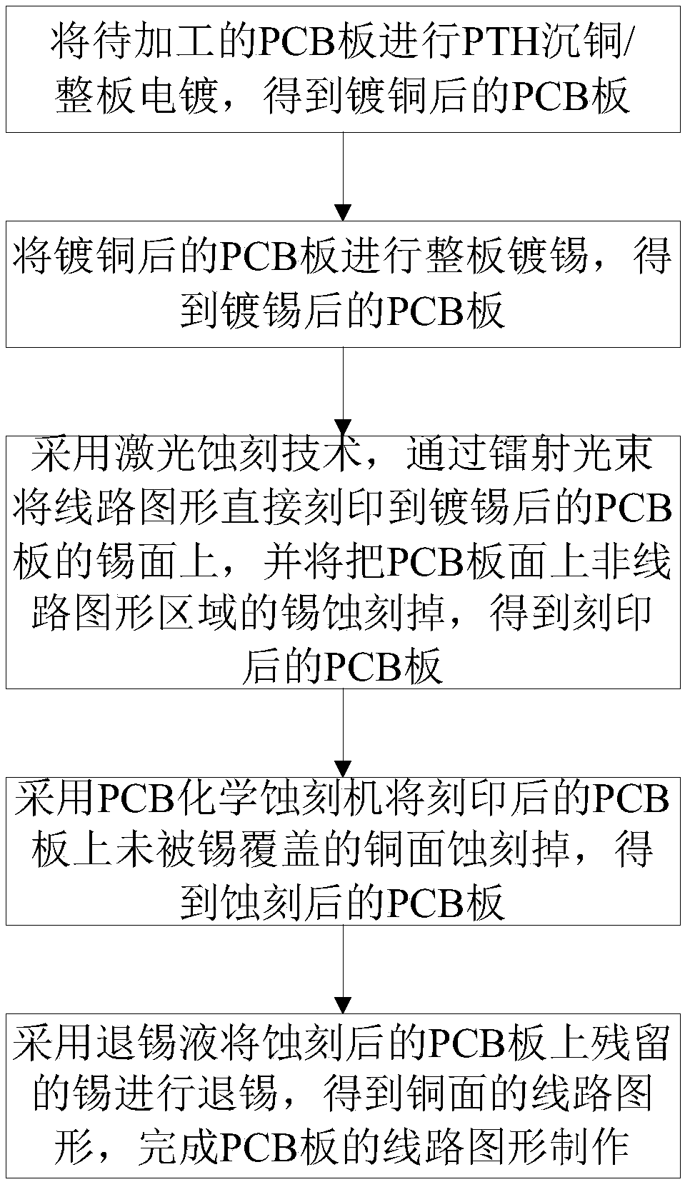
Method for manufacturing PCB circuit pattern
A technology of PCB boards and circuit graphics, applied in the fields of printed circuit manufacturing, printed circuits, electrical components, etc., can solve the problems of endless development, increased input costs, and increased production of defective products, so as to simplify the production process and reduce input costs Effect
- Summary
- Abstract
- Description
- Claims
- Application Information
AI Technical Summary
Problems solved by technology
Method used
Image

Examples
Embodiment Construction
[0033] It should be noted that, in the case of no conflict, the embodiments in the present application and the features in the embodiments can be combined with each other. The present invention will be further described in detail below in conjunction with the drawings and specific embodiments.
[0034] If there are directional indications (such as up, down, left, right, front, back...) in the embodiments of the present invention, they are only used to explain the relative positions of the components in a certain posture (as shown in the drawings) relationship, motion, etc., if the particular pose changes, the directional indication changes accordingly.
[0035] In addition, in the present invention, the descriptions involving "first", "second" and so on are only for the purpose of description, and should not be understood as indicating or implying their relative importance or implicitly indicating the quantity of the indicated technical features. Thus, the features defined as ...
PUM
 Abstract
Description
Claims
Application Information