Silicon wafer molding processing method

A molding process, silicon wafer technology, applied in stone processing equipment, metal processing equipment, manufacturing tools, etc., can solve the problems of low production efficiency, cumbersome processing process, difficulty in meeting the requirements of various indicators of silicon wafers, etc., and achieve high processing efficiency , good quality, avoid cutting time-consuming effect

Inactive Publication Date: 2019-12-31
XIAN ESWIN MATERIAL TECH CO LTD +1
View PDF10 Cites 8 Cited by
  • Summary
  • Abstract
  • Description
  • Claims
  • Application Information

AI Technical Summary

Problems solved by technology

[0003] In view of this, the present invention provides a method for molding and processing silicon wafers to solve the problems of cumbersome processing, low production efficiency, and difficulty in meeting the requirements of various indicators of the produced silicon wafers.

Method used


Image

  • Silicon wafer molding processing method
  • Silicon wafer molding processing method
  • Silicon wafer molding processing method

Examples


Embodiment Construction

[0035] In order to make the purpose, technical solutions and advantages of the embodiments of the present invention more clear, the following will clearly and completely describe the technical solutions of the embodiments of the present invention in conjunction with the drawings of the embodiments of the present invention. Apparently, the described embodiments are some, not all, embodiments of the present invention. All other embodiments obtained by those skilled in the art based on the described embodiments of the present invention belong to the protection scope of the present invention.

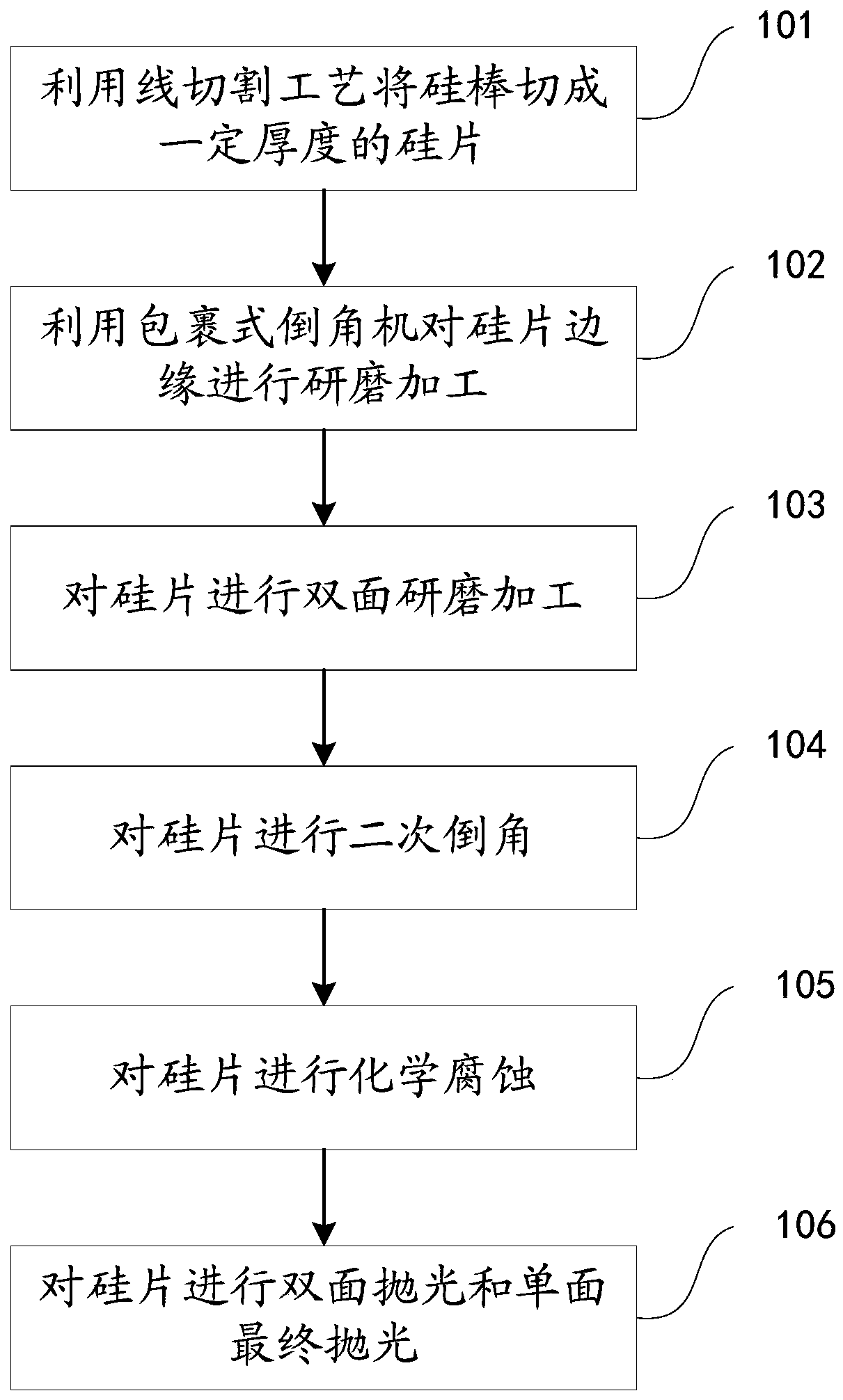
[0036] Such as figure 1 As shown, the existing silicon wafer processing technology mainly includes the following steps:

[0037] Step 101: cutting the silicon rod into silicon wafers with a certain thickness by wire cutting process.

[0038] In step 101, the silicon rod is usually cut into silicon wafers of a certain thickness by wire cutting. At the same time, the mortar is sprayed on t...


PUM

PropertyMeasurementUnit
diameteraaaaaaaaaa
thicknessaaaaaaaaaa
surface roughnessaaaaaaaaaa

Abstract

The invention provides a silicon wafer molding processing method. The silicon wafer molding processing method comprises the following steps of cutting a silicon rod into a silicon wafer by adopting amulti-line acid corrosion cutting process; chamfering the silicon wafer; grinding the surface of the silicon wafer after chamfering; and polishing the ground silicon wafer after grinding. According tothe silicon wafer forming processing method, the silicon rod is cut by adopting a multi-line acid corrosion cutting process, the ultrathin silicon wafer can be obtained, the processing efficiency ishigh, the quality is good, the various reaction rates are controllable, the problems that the silicon wafer is long in cutting time and large in noise in the traditional silicon wafer forming processing process, and the quality of the silicon wafer obtained by cutting cannot meet the requirements are solved.

Description

technical field [0001] The invention relates to the technical field of silicon wafer processing, in particular to a silicon wafer forming and processing method. Background technique [0002] Silicon wafer is an important base material in the semiconductor field. With the continuous improvement of chip manufacturing and technology, especially the chip technology has entered the line width process of 7nm, 5nm or even lower, higher requirements are put forward for the processing and quality of silicon wafers. Require. However, the existing silicon wafer molding process mainly includes slicing, primary chamfering, double-sided grinding, secondary chamfering, chemical corrosion, double-sided polishing, and final single-sided polishing. The process is cumbersome and complicated, with many types of equipment and low production efficiency. The warpage, local surface flatness, and surface roughness of the silicon wafers that come out cannot meet the requirements. Contents of the i...

Claims


Application Information

Patent Timeline
Patent Type & Authority Applications(China)
IPC IPC(8): B28D5/04B28D7/00B24B9/06B24B27/06B24B37/08B24B57/02H01L21/02
CPCB24B9/065B24B27/0633B24B37/08B24B57/02B28D5/007B28D5/045H01L21/02013
Inventor 陈兴松
Owner XIAN ESWIN MATERIAL TECH CO LTD
Why Eureka
Try Eureka