Focal plane detector suitable for curved surface imaging and preparation method of detector
A technology of focal plane detector and focal plane array, which is applied in the direction of electric radiation detector, radiation pyrometry, instrument, etc., and achieves the effect of simple preparation process, high preparation efficiency and convenient peeling
- Summary
- Abstract
- Description
- Claims
- Application Information
AI Technical Summary
Problems solved by technology
Method used
Image
Examples
Embodiment 1
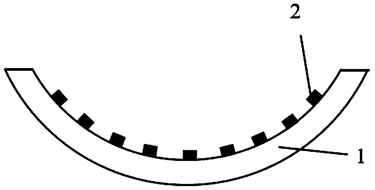
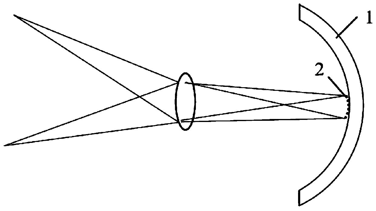
[0019] Taking the pixel pitch as 15 μm, the silicon-based chip array as 640×512, the F-number as 0.9, and the focal length as 20mm as examples, the structure of the present invention and the specific implementation of the preparation method will be further described in conjunction with the accompanying drawings:
[0020] The silicon-based chip is prepared on the silicon oxide layer or other sacrificial layer. After the preparation is consistent with the normal process, the silicon-based chip on the sacrificial layer can be obtained. After the sacrificial layer is completely removed, the upper silicon-based chip can be peeled off to form a A flexible silicon-based thin layer, the thin layer thickness is 0.01mm, the silicon-based thin layer is bonded to the supporting substrate with DW-3 low-temperature epoxy glue. The silicon nitride material is then placed on a PDMS flexible mold with a certain curvature to shape it. The PDMS flexible mold in this example is a hemispherical mol...
Embodiment 2
[0022] Taking the pixel pitch as 15 μm, the silicon-based chip array as 640×512, the F-number as 2, and the focal length as 60mm as examples, the structure of the present invention and the specific implementation of the preparation method will be further described in conjunction with the accompanying drawings:
[0023] The silicon-based chip is prepared on the silicon oxide layer or other sacrificial layer. After the preparation is consistent with the normal process, the silicon-based chip on the sacrificial layer can be obtained. After the sacrificial layer is completely removed, the upper silicon-based chip can be peeled off to form a A flexible silicon-based thin layer, the thin layer thickness is 0.05mm, the silicon-based thin layer is bonded to the supporting substrate with DW-3 low-temperature epoxy glue, and the supporting substrate is 0.2mm thick in this example. The silicon nitride material is then placed on a PDMS flexible mold with a certain curvature, and shaped. Th...
Embodiment 3
[0025] Taking the pixel pitch as 15 μm, the silicon-based chip array as 640×512, the F number as 5, and the focal length as 150 mm as examples, the structure of the present invention and the specific implementation of the preparation method will be further described in conjunction with the accompanying drawings:
[0026] The silicon-based chip is prepared on the silicon oxide layer or other sacrificial layer. After the preparation is consistent with the normal process, the silicon-based chip on the sacrificial layer can be obtained. After the sacrificial layer is completely removed, the upper silicon-based chip can be peeled off to form a A flexible silicon-based thin layer, the thin layer thickness is 0.1mm, the silicon-based thin layer is bonded to the supporting substrate with DW-3 low-temperature epoxy glue, and the supporting substrate is 0.5mm thick in this example The silicon nitride material is then placed on a PDMS flexible mold with a certain curvature, and shaped. Th...
PUM
| Property | Measurement | Unit |
|---|---|---|
| Thickness | aaaaa | aaaaa |
Abstract
Description
Claims
Application Information

