SIP packaging method for realizing electromagnetic shielding

A packaging method and electromagnetic shielding technology, applied in circuits, electrical components, electrical solid devices, etc., can solve the problems of increasing the size of the connection between the PCB board and the SIP module, unfavorable miniaturization trends, etc., to save packaging space size, improve flexibility properties, and the effect of improving impact strength

Inactive Publication Date: 2019-12-31
苏州中科安源信息技术有限公司 +1
View PDF5 Cites 0 Cited by
  • Summary
  • Abstract
  • Description
  • Claims
  • Application Information

AI Technical Summary

Problems solved by technology

[0004] The traditional solution to external radiation is to metallize the surface of SIP (System In a Package) module products. Although this solution slows down the radiation interference of the external electromagnetic environment on the SIP internal chip to a certain extent, it increases the The size of the connection between the PCB board and the SIP module is not conducive to the final miniaturization trend of the product

Method used


Image

  • SIP packaging method for realizing electromagnetic shielding

Examples


Embodiment Construction

[0014] In order to better illustrate the working mode of the present invention, the present invention will be described in detail with completeness and clarity below in conjunction with specific drawings.

[0015] A SIP encapsulation method for realizing electromagnetic shielding, specifically as follows:

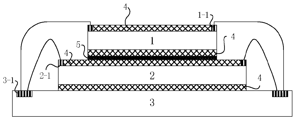
[0016] Such as figure 1 As shown, the hardware of the present invention includes a high-capacity Flash storage chip 1, a MCU chip 2, and a substrate 3 to form a high-storage chip system, which effectively overcomes the insufficient data storage space of the MCU chip.

[0017] Firstly, the upper and lower surfaces of the Flash memory chip 1 and the MCU chip 2 are coated with an absorbing material to form a shielding layer 4 . The edge pins 1-1 of the Flash memory chip 1 and the edge pins 2-1 of the MCU chip 2 are not painted. Shielding layer 4 thickness is 25~100 μ m (the present embodiment adopts 50 μ m), and the absorbing material that adopts is graphene, and graphene is...


PUM


Abstract

The invention discloses a SIP packaging method for realizing electromagnetic shielding. Surface metallization is adopted traditionally to prevent radiation interference, and a size of module connection is increased. The method comprises the steps that firstly, upper and lower surfaces of an MCU chip and a Flash storage chip in an SIP module are smeared with absorbing materials in a full-surface mode to form a shielding layer, and the adopted absorbing materials are graphene; the MCU chip and the Flash memory chip are connected by adopting an SPI bus so as to communicate with each other by adopting an up-and-down laminated packaging method; and then the MCU chip is connected with a substrate in a forward bonding mode, and the Flash memory chip is connected with the substrate in a reverse bonding mode. By using the method, electromagnetic waves can be effectively absorbed, an electromagnetic field permeating into the chip is reduced, signal transmission quality is improved, and an EMI problem is reduced. And a lead is bonded in a reverse manner so that a height of stacked packaging can be effectively reduced.

Description

technical field [0001] The invention belongs to the technical field of chips, in particular to the technical field of chip packaging, and relates to a SIP packaging method for realizing electromagnetic shielding. Background technique [0002] With the further improvement of the integration level of two-dimensional integrated circuits, the semiconductor industry is approaching the bottleneck of the expansion of transistors, and three-dimensional (3D) integration technology is regarded as a promising solution to extend Moore's law for the next generation of semiconductor technology . Chip stack packaging is a three-dimensional encapsulation technology, which can integrate functional chips such as processors, memory chips, and encryption chips into one package to achieve a complete function, making integrated circuits continue to be miniaturized, high-performance, and high-end. Integration and low-cost development. [0003] However, new applications place new demands on the e...

Claims


Application Information

Patent Timeline
Patent Type & Authority Applications(China)
IPC IPC(8): H01L25/065H01L23/31H01L23/60H01L21/56H01L23/48
CPCH01L25/0652H01L23/3121H01L23/60H01L21/561H01L23/481H01L2224/48471H01L2224/73265H01L2224/32145
Inventor 姜显扬陈木市王德富徐欣
Owner 苏州中科安源信息技术有限公司
Why Eureka
Try Eureka