SSD stacked packaging structure and preparation method thereof

A packaging structure and mounting technology, applied in semiconductor/solid-state device manufacturing, semiconductor/solid-state device components, semiconductor devices, etc., can solve problems such as the large volume of SSD stacking packages, achieve low cost, reduce pressure, and prevent splitting Effect

Inactive Publication Date: 2019-12-31
HUATIAN TECH XIAN
View PDF6 Cites 0 Cited by
  • Summary
  • Abstract
  • Description
  • Claims
  • Application Information

AI Technical Summary

Problems solved by technology

[0005] The purpose of the present invention overcomes the shortcomings of the large volume of SSD stack package

Method used


Image

  • SSD stacked packaging structure and preparation method thereof
  • SSD stacked packaging structure and preparation method thereof
  • SSD stacked packaging structure and preparation method thereof

Examples


preparation example Construction

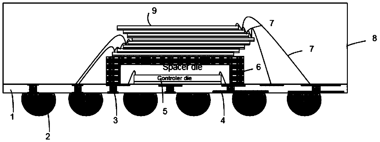
[0047] The method for preparing the above-mentioned SSD stack package structure includes the following steps:

[0048] An accommodating space is formed on the lower surface of the spacer 6;

[0049] Mounting a control chip 5 on the substrate 1 to electrically connect the control chip 5 to the substrate 1;

[0050] Mount the spacer 6 with the accommodation space on the substrate 1, and place the control chip 5 in the accommodation space;

[0051] Mounting the memory chip 9 on the upper surface of the spacer 6;

[0052] The spacer 6 is mounted on the substrate 1, and the control chip 5 is placed in the accommodating space; the circuit connection is realized by wire bonding;

[0053] Finally, the plastic package 8 wraps the substrate 1 , the spacer 6 , the memory chip 9 and the bonding wire 7 for plastic packaging.

[0054] The spacer 6 is etched and grooved to form an accommodating space of a U-shaped groove structure.

Embodiment

[0056] Figure 2 to Figure 4 It is the packaging structure manufacturing method of some embodiments of the present invention, and the specific manufacturing method is as follows:

[0057] figure 2 It is a schematic diagram of forming a U-shaped groove by etching and grooving, and then cutting to form a separate spacer. The material of the spacer is not limited, such as silicon material, and mainly plays a supporting role; when the spacer 6 is made of metal, the number of control chips 5 can be reduced. electromagnetic interference, and at the same time strengthen the heat dissipation of the upper stacked memory chips 9 .

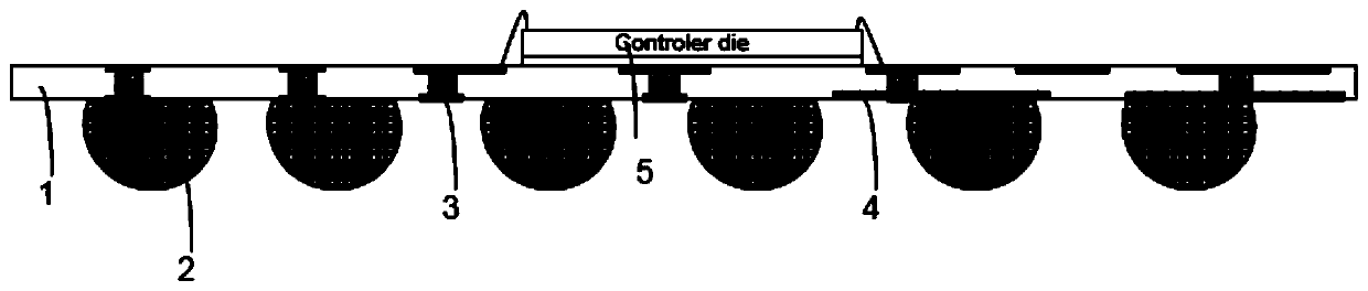
[0058] image 3 It is to provide a core on the substrate 1; mount the control chip 5 on the substrate 1;

[0059] Figure 4 exist image 3 On the basis of the secondary core (upper spacer); the spacer 6 is mounted on the substrate 1, and the control chip 5 is placed in the accommodating space;

[0060] Figure 5 is in Figure 4On the basis of adding...


PUM


Abstract

The invention discloses an SSD stacked packaging structure and a preparation method thereof. The SSD stacked packaging structure is characterized by comprising a substrate; a control chip which is surface-mounted on the substrate and electrically connected with the substrate; a spacer of which the lower surface is provided with an accommodating space, wherein the spacer is surface-mounted on the substrate, and the control chip is arranged in the accommodating space; a memory chip which is surface-mounted on the upper surface of the spacer and electrically connected with the substrate through abonding wire; and a plastic packaging body which covers the substrate, the spacer, the memory chip and the bonding wire. According to the packaging structure, the control chip is protected from cracking through the U-shaped Spacer, and the packaging structure is small in size and easy to implement and improves the packaging quality.

Description

technical field [0001] The invention belongs to the technical field of storage chip packaging, and relates to an SSD stack packaging structure and a preparation method thereof. Background technique [0002] The trend of SSD (Solid State Drives) stacked packaging is thin package, small volume, high integration, and large capacity. For ultra-thin chip packaging, the reliability and high integration of multi-chip stacking have become a major trend in packaging. This is the A challenge for industry technologists. [0003] For SSD packaging, the control chip and the storage chip are usually packaged together. At present, there are three types of SSD packaging: 1. The control chip is placed on one side alone, and the memory chip is placed on the other side; 2. The control chip is placed on the bottom layer, and the storage chip is laminated on the top; [0004] At present, these three kinds of problems exist respectively: 1. It is easy to implement and has a large volume; 2. The...

Claims


Application Information

Patent Timeline
IPC IPC(8): H01L25/065H01L25/18H01L23/31H01L21/98
CPCH01L25/0657H01L25/18H01L25/50H01L23/3128H01L2224/32225H01L2224/32145H01L2224/48145H01L2224/48227H01L2224/73265H01L2924/00012
Inventor 王蕊熊涛马晓建
Owner HUATIAN TECH XIAN
Why Eureka
Try Eureka