Miniled backlight substrate packaging method

A packaging method and substrate technology, applied in electrical components, circuits, semiconductor devices, etc., can solve the problems of volatilization of solvents, affecting visual experience, difficulty, etc., to solve cross-light diffraction, avoid bonding failure, and increase backlight. effect of brightness

Active Publication Date: 2019-12-31
美琪电路江门有限公司
View PDF7 Cites 1 Cited by
  • Summary
  • Abstract
  • Description
  • Claims
  • Application Information

AI Technical Summary

Problems solved by technology

At present, the minimum gap of ordinary silver paste or tin paste can only achieve the placement with a positive and negative gap of 50 μm, and it is very difficult, which may easily cause a micro-short circuit between the positive and negative electrodes
[0003] The number of Miniled backlight substrate chips is huge. For the traditional silver paste and solder paste process, during production, due to the long time of solid crystal, the solvent of the paste is easy to volatilize, resulting in the failure of placement
[0004] In addition, the brightness loss of the backlight substrate in the prior art is very large, and there is a problem of light diffraction, which cannot block light, which affects the visual experience

Method used


Image

  • Miniled backlight substrate packaging method
  • Miniled backlight substrate packaging method
  • Miniled backlight substrate packaging method

Examples


Embodiment Construction

[0042] Below, the present invention will be further described in conjunction with the accompanying drawings and specific implementation methods. It should be noted that, under the premise of not conflicting, the various embodiments described below or the technical features can be combined arbitrarily to form new embodiments. .

[0043] A miniled backlight substrate packaging method, comprising the following steps:

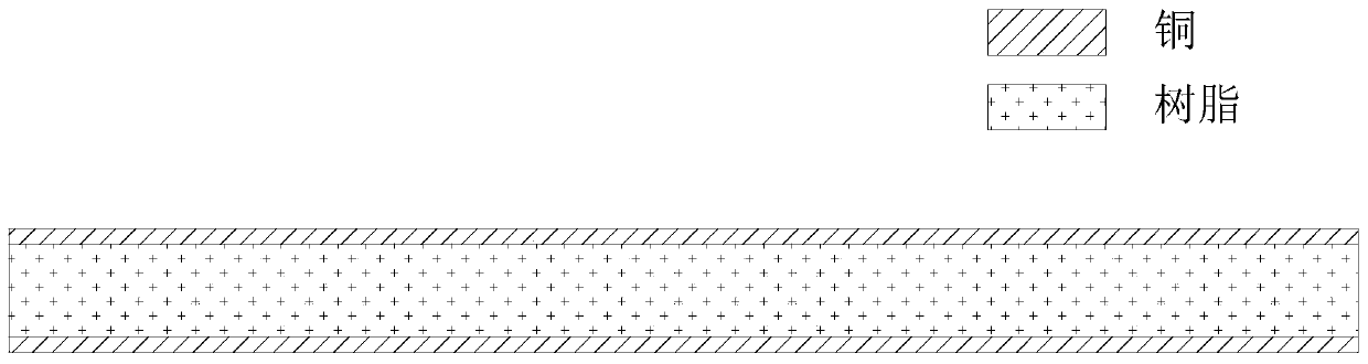
[0044] Material preparation steps (combined with figure 1 ): preparing a double-sided copper-clad laminate, the thickness of the double-sided copper-clad laminate is 100-1000 μm, and the thickness of the single-layer copper foil is 12-35 μm. Specifically, the resin layer of the double-sided copper clad laminate is BT resin. Specifically, the double-sided copper-clad laminate is an FR4 double-sided copper-clad laminate with a Tg value greater than 150 degrees Celsius.

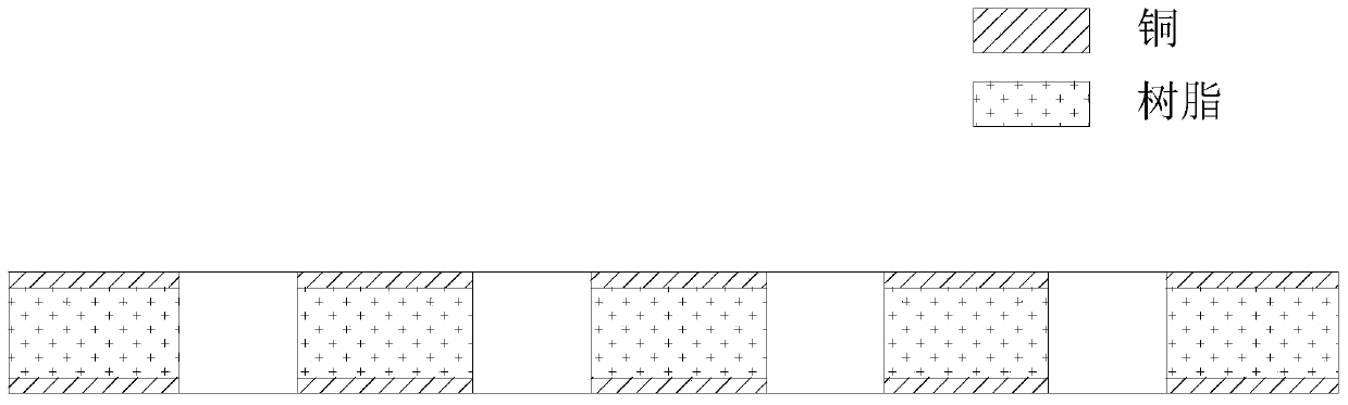
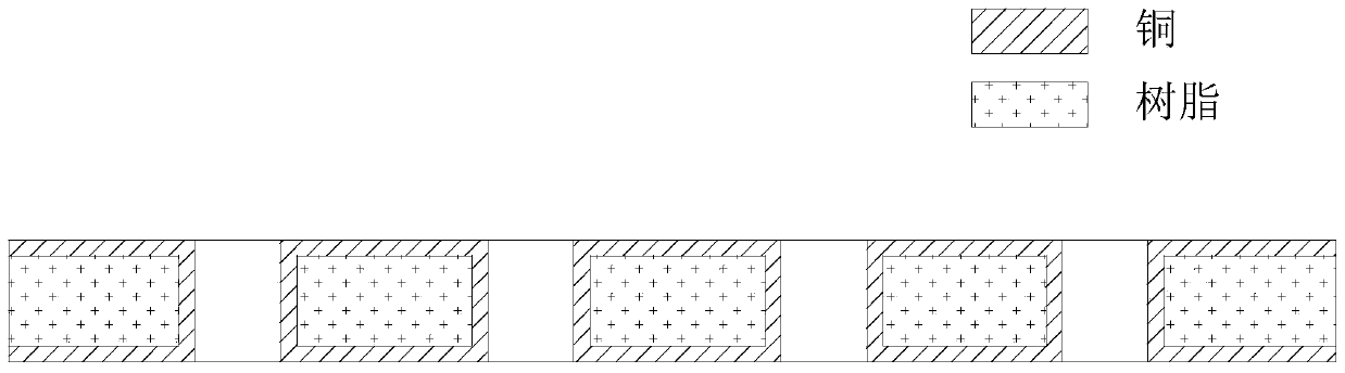
[0045] Drilling steps (combined with figure 2 ): Drill holes on the double-sided copper-clad...


PUM

PropertyMeasurementUnit
thicknessaaaaaaaaaa
thicknessaaaaaaaaaa
diameteraaaaaaaaaa

Abstract

A miniled backlight substrate packaging method comprises the following steps: the step of material preparation: preparing a double-sided copper-clad plate, wherein the thickness of the double-sided copper-clad plate is 100-1000 micrometers, the thickness of a single layer of copper foil being 12-35 micrometers; the step of drilling: drilling the double-sided copper-clad plate to ensure that drilled holes run through two layers of copper foils of the double-sided copper-clad plate; the step of copper plating: plating copper on the walls of the drilled holes of the double-sided copper-clad plateto make the copper plating layers on the walls of the drilled holes connected with the copper foils on the two sides of the double-sided copper-clad plate to allow the copper foils on the two sides of the double-sided copper-clad plate to be electrically connected; and the step of hole filling: filling the drilled holes with white resin or white ink. The white resin used in the anisotropic conductive adhesive manufacturing step is melted, and the side faces of a miniled chip is wrapped due to surface tension, so that the chip is independently wrapped, a reflection cup is formed, and the reflection brightness of light is improved.

Description

technical field [0001] The invention relates to a miniled backlight substrate packaging method. Background technique [0002] The specifications of flip chips are getting smaller and smaller, and the gap between positive and negative electrodes is as small as 20 μm. At present, the minimum gap of ordinary silver paste or tin paste can only realize the placement with a gap of 50 μm between the positive and negative electrodes, and it is very difficult, which may easily cause a micro-short circuit between the positive and negative electrodes. [0003] The number of Miniled backlight substrate chips is huge. For the traditional silver paste and solder paste process, during production, due to the long time of solid crystal, the solvent of the paste is easy to volatilize, resulting in the failure of placement. [0004] In addition, the brightness loss of the backlight substrate in the prior art is large, and there is a problem of light diffraction, which cannot block light and a...

Claims


Application Information

Patent Timeline
Patent Type & Authority Applications(China)
IPC IPC(8): H01L33/62H01L33/60H01L33/56H01L33/48
CPCH01L33/48H01L33/56H01L33/60H01L33/62H01L2933/0033H01L2933/005H01L2933/0058H01L2933/0066
Inventor 康孝恒蔡克林李瑞许凯
Owner 美琪电路江门有限公司
Why Eureka
Try Eureka