Manufacturing method of silicon epitaxial wafer for 8-inch VDMOS power tube

A technology of silicon epitaxial wafers and manufacturing methods, applied in semiconductor/solid-state device manufacturing, electrical components, circuits, etc., can solve problems such as uneven resistivity of epitaxial layers, achieve improved impurity distribution, increase yield, and reduce transition zone width Effect

Active Publication Date: 2020-01-07
NANJING GUOSHENG ELECTRONICS
View PDF5 Cites 3 Cited by
  • Summary
  • Abstract
  • Description
  • Claims
  • Application Information

AI Technical Summary

Problems solved by technology

[0005] Purpose of the invention: In view of the above problems, the present invention proposes a method for manufacturing silicon epitaxial wafers for 8-inch VDMOS power tubes to solve the problem of inhomogeneous resistivity of the epitaxial layer of epitaxial wafers for 8-inch VDMOS power tubes

Method used


Image

  • Manufacturing method of silicon epitaxial wafer for 8-inch VDMOS power tube
  • Manufacturing method of silicon epitaxial wafer for 8-inch VDMOS power tube

Examples


Embodiment Construction

[0022] The technical solutions of the present invention will be further described below in conjunction with the accompanying drawings and embodiments.

[0023] The manufacture method of 8 inches VDMOS power tube silicon epitaxial wafers of the present invention, comprises the following steps:

[0024] (1) As-doped substrate is selected, and the resistivity is ≤0.004Ω.cm; the back of the substrate is made of silicon dioxide (LTO) + polysilicon (Poly) back seal; the edge width of the back seal layer is 0.4~0.9mm.

[0025] The substrate is chamfered and polished to reduce the crystal points on the back and improve the local flatness.

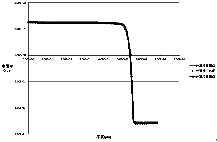
[0026] The substrate is baked at high temperature for a period of time before epitaxy to reduce the self-doping during epitaxy growth. The baking temperature before epitaxy is 1090~1130℃, and the baking time is more than 5min.

[0027] (2) To grow the first epitaxial layer, grow the first epitaxial layer on the surface of the high-concentration su...


PUM

PropertyMeasurementUnit
electrical resistivityaaaaaaaaaa

Abstract

The invention discloses a manufacturing method of a silicon epitaxial wafer for an 8-inch VDMOS power tube, which comprises the steps of (1) selecting an As-doped substrate, wherein the resistivity ofthe substrate is less than or equal to 0.004 omega.cm; (2) growing a first epitaxial layer, wherein the first epitaxial layer grows on the surface of the substrate at the growth temperature of 1040-1080 DEG C and the growth rate of less than or equal to 1.5[mu]m/min, and purging the cavity with hydrogen after the growth of the first epitaxial layer is completed; and (3) and growing a second epitaxial layer, wherein second epitaxial layer grows on the surface of the first epitaxial layer at the growth temperature of 1040-1060 DEG C and the growth rate of 2-3[mu]m/min. According to the invention, the proper substrate is selected, the device and epitaxial requirements are met, the resistivity uniformity of the epitaxial layer is effectively improved, the deviation between the edge and the central region transition region is reduced, and the yield of the die is improved.

Description

technical field [0001] The invention relates to a method for manufacturing an epitaxial wafer, in particular to a method for manufacturing a silicon epitaxial wafer for an 8-inch VDMOS power tube. Background technique [0002] The MOSFET power tube is a voltage-controlled unipolar transistor that controls the drain current through the gate voltage. The fine processing technology of VLSI is adopted, and the N / N+ epitaxial structure is used, so there are special requirements and standards for epitaxial wafers. [0003] The epitaxial wafer for 8-inch VDMOS power tube has higher requirements on the uniformity of surface resistivity and the longitudinal distribution of resistivity because its surface area is 1.78 times that of the 6-inch epitaxial wafer. The epitaxial wafer material for VDMOS power tube requires the uniformity of resistivity in the flat area of ​​the surface to be ≤6%, and the transition area to be less than 1μm. Due to the influence of self-doping, it is diffi...

Claims


Application Information

Patent Timeline
Patent Type & Authority Applications(China)
IPC IPC(8): H01L21/02H01L29/78
CPCH01L21/02381H01L21/02532H01L21/02576H01L21/02612H01L21/02656H01L29/7802
Inventor 马梦杰
Owner NANJING GUOSHENG ELECTRONICS
Why Eureka
Try Eureka