A crimping type power switch module and preparation method thereof

A power switch module and power switch chip technology, which is applied in the direction of output power conversion devices, semiconductor/solid-state device parts, semiconductor devices, etc., can solve the problems of high chip current density and device failure, and achieve improved current sharing performance, The effect of increasing the safe working area and reducing the mutual inductance parameters

Active Publication Date: 2021-09-24
SOUTH UNIVERSITY OF SCIENCE AND TECHNOLOGY OF CHINA
View PDF5 Cites 0 Cited by
  • Summary
  • Abstract
  • Description
  • Claims
  • Application Information

AI Technical Summary

Problems solved by technology

The electromagnetic interference of the conductive path of each sub-module is very strong, which will cause serious current inhomogeneity, and the current of the external chip will be greater than that of the internal chip
As a result, the current density of some chips is too high. When the device is in a critical working state, some chips may have been overloaded, and device failure is very prone to occur.

Method used


Image

  • A crimping type power switch module and preparation method thereof
  • A crimping type power switch module and preparation method thereof
  • A crimping type power switch module and preparation method thereof

Examples


Embodiment 1

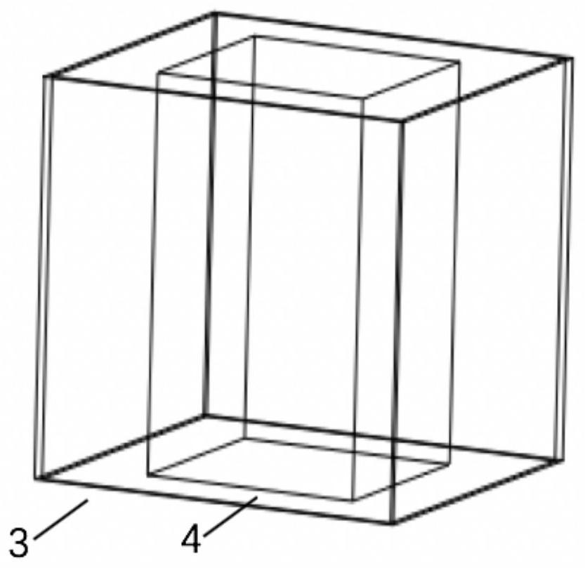
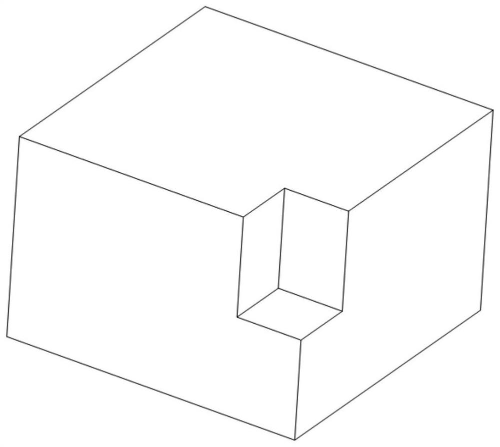
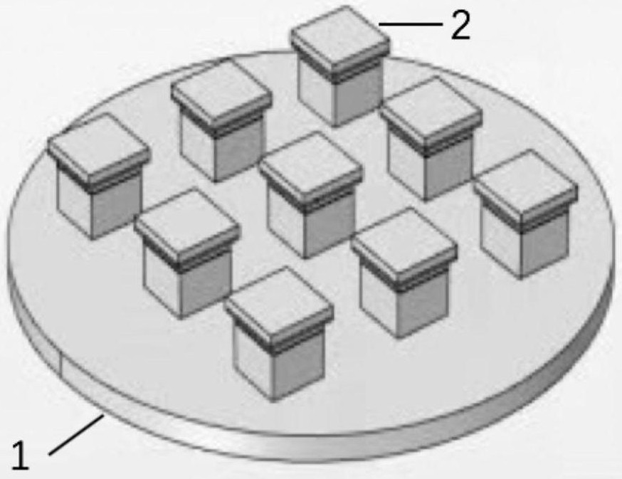
[0031] This embodiment provides a crimping type power switch module, such as Figure 1-6 As shown, it includes: an upper end plate, a lower end plate 1, a PCB board, and at least one subunit 2 between the upper end plate and the lower end plate. The subunit includes: a supporting frame 3, and a bottom-up The set conductive metal sheet, the first molybdenum sheet, the power switch chip, and the second molybdenum sheet; the support frame includes a metal frame and an insulating layer wrapped outside the metal frame.

[0032] The thickness of the metal frame is 2mm-4mm; the thickness of the insulating layer is at least 2mm, and the upper and lower gaps do not exceed 2mm; the distance between the support frame and the power switch chip is 4mm-8mm. Different surface thicknesses and structures need to be uniformly set, and the shielding effect of the grid is relatively poor compared to the plate type.

[0033] The material of the metal frame is a highly conductive metal material, s...


PUM


Abstract

A crimping type power switch module, characterized in that it includes: an upper end plate, a lower end plate, a PCB board, and at least one subunit between the upper end plate and the lower end plate, the subunit includes: a supporting frame, and a The conductive metal sheet, the first molybdenum sheet, the power switch chip, and the second molybdenum sheet are arranged from bottom to top inside the support frame; the support frame includes a metal frame and an insulating layer wrapped outside the metal frame. The invention avoids the technical problem of severe current interference between multiple bullet element chips in the crimping device, increases the safe working area of ​​the power device, and improves the current equalization performance among each bullet element.

Description

technical field [0001] The field of semiconductor packaging, specifically related to the packaging technology of power electronic devices Background technique [0002] Inside the traditional soldered IGBT, the stray parameters of the line are relatively large, and a large voltage spike will be generated during the turn-off process accompanied by certain electromagnetic interference. When the power system puts forward higher requirements on the power level and requires more chips to be connected in parallel, the parasitic parameters and differences of the chip gate, emitter, and collector will be further increased, which will aggravate the voltage overshoot and increase the Switching losses, and lead to large current imbalance, thereby reducing the reliability of the device. Compared with the soldered IGBT, the crimped IGBT has the advantages of high voltage, high current, low stray inductance, fast switching speed, and double-sided heat dissipation. Therefore, the crimped I...

Claims


Application Information

Patent Timeline
Patent Type & Authority Patents(China)
IPC IPC(8): H01L23/31H01L23/552H01L25/11H02M1/00
CPCH01L23/31H01L23/552H01L25/11H02M1/00
Inventor 刘洋敖日格力叶怀宇刘旭
Owner SOUTH UNIVERSITY OF SCIENCE AND TECHNOLOGY OF CHINA
Why Eureka
Try Eureka