Enhanced field effect transistor

A field-effect transistor and enhanced technology, which is applied in the direction of semiconductor devices, electrical components, circuits, etc., can solve the problems of poor reliability, small breakdown voltage, and easy damage, and achieve the effect of improving reliability and breakdown voltage

Active Publication Date: 2020-01-10
THE 13TH RES INST OF CHINA ELECTRONICS TECH GRP CORP
View PDF14 Cites 0 Cited by
  • Summary
  • Abstract
  • Description
  • Claims
  • Application Information

AI Technical Summary

Problems solved by technology

[0004] In view of this, an embodiment of the present invention provides an enhancement type field effect transistor to solve the problems of low breakdown voltage, easy damage and poor reliability of the enhancement type field effect transistor realized in the prior art

Method used


Image

  • Enhanced field effect transistor
  • Enhanced field effect transistor
  • Enhanced field effect transistor

Examples


Embodiment Construction

[0027] In the following description, specific details such as specific system structures and technologies are presented for the purpose of illustration rather than limitation, so as to thoroughly understand the embodiments of the present application. It will be apparent, however, to one skilled in the art that the present application may be practiced in other embodiments without these specific details. In other instances, detailed descriptions of well-known systems, devices, circuits, and methods are omitted so as not to obscure the description of the present application with unnecessary detail.

[0028] In order to illustrate the technical solutions of the present invention, specific examples are used below to illustrate.

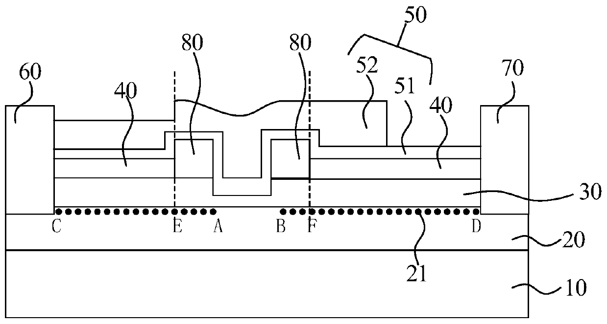
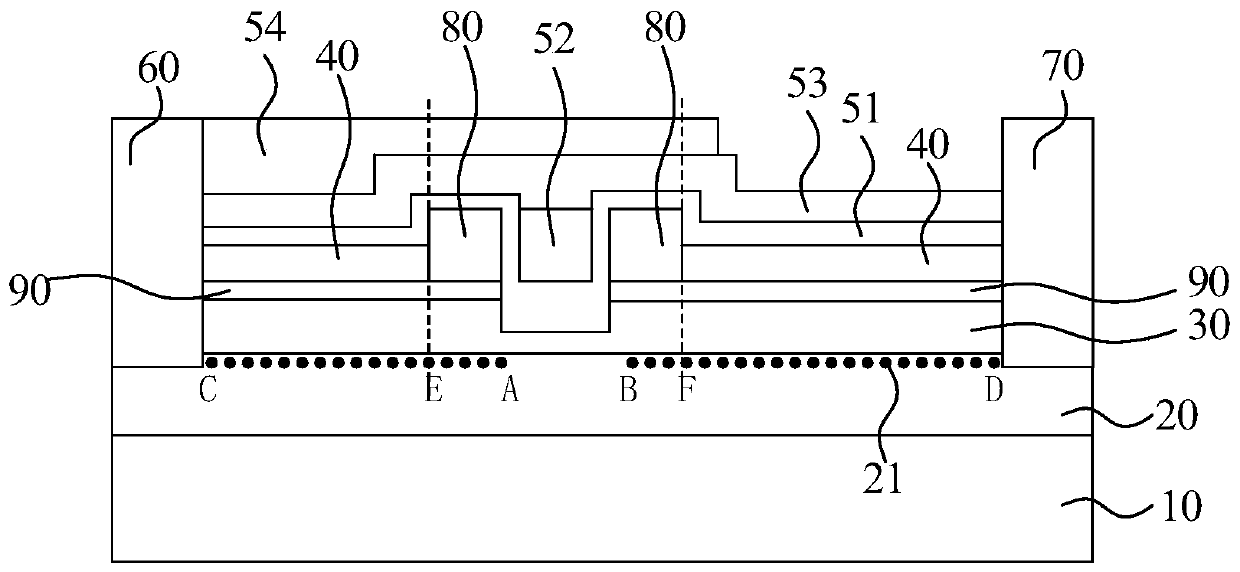
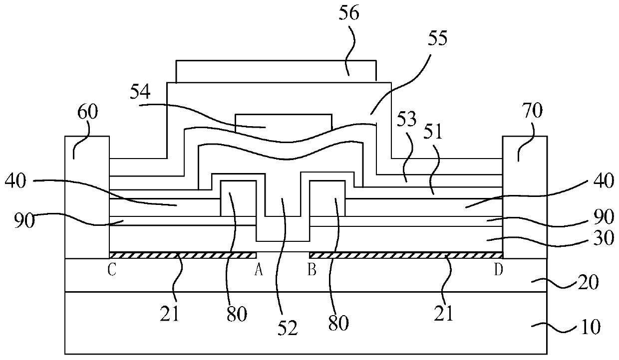
[0029] figure 1 It is a schematic structural diagram of an enhancement field effect transistor provided by an embodiment of the present invention. For convenience of description, only the parts related to the embodiment of the present invention are shown....


PUM

PropertyMeasurementUnit
Thicknessaaaaaaaaaa
Thicknessaaaaaaaaaa
Thicknessaaaaaaaaaa

Abstract

The invention is applicable to the technical field of semiconductor devices, and discloses an enhanced field effect transistor. The enhanced field effect transistor sequentially comprises a substrate,a channel layer, a barrier layer, a passivation layer and at least one layer of preset structure from bottom to top. The preset structure sequentially comprises an insulating dielectric layer and a field plate from bottom to top. A source electrode and a drain electrode are arranged on the channel layer. A gate electrode is arranged on the barrier layer. The passivation layer is positioned between the source electrode and the gate electrode and between the gate electrode and the drain electrode. The insulating dielectric layer covers the gate electrode. A carrier-free region and a carrier region exist in the channel layer between the source electrode and the drain electrode, a carrier-free region exists in the channel layer except the part right below the gate electrode, and a carrier region exists in the channel layer right below the gate electrode. The field plate is arranged right above the carrier-free regions. According to the enhanced field effect transistor provided by the invention, an enhanced device is realized by using transverse energy band engineering, and the breakdown voltage can be increased and the reliability of the device can be improved by using the field platestructure.

Description

technical field [0001] The invention belongs to the technical field of semiconductor devices, in particular to an enhanced field effect transistor. Background technique [0002] Field effect transistors are referred to as field effect transistors, which have the advantages of high input resistance, low noise, low power consumption, large dynamic range, easy integration, no secondary breakdown phenomenon, and wide safe working area. One of the working modes of field effect transistors is enhancement mode. [0003] At present, enhancement-mode field-effect transistors are usually realized based on vertical energy band engineering, but the breakdown voltage of enhancement-mode field-effect transistors realized in this way is small, easy to damage, and poor in reliability. Contents of the invention [0004] In view of this, an embodiment of the present invention provides an enhancement type field effect transistor to solve the problems of low breakdown voltage, easy damage an...

Claims


Application Information

Patent Timeline
IPC IPC(8): H01L29/778H01L29/40
CPCH01L29/7787H01L29/407Y02B70/10
Inventor 王元刚冯志红吕元杰宋旭波谭鑫周幸叶房玉龙尹甲运
Owner THE 13TH RES INST OF CHINA ELECTRONICS TECH GRP CORP
Why Eureka
Try Eureka