High-power power supply backplane for high density assembling
A high-power, high-density technology, applied in the fields of electrical engineering and equipment power generation, power transformation or power distribution, can solve problems such as low maintainability, low PDU power, chaotic wiring, etc., to simplify power distribution installation work Quantity, conducive to large-scale construction, power and guaranteed effect
- Summary
- Abstract
- Description
- Claims
- Application Information
AI Technical Summary
Problems solved by technology
Method used
Image
Examples
Embodiment 1
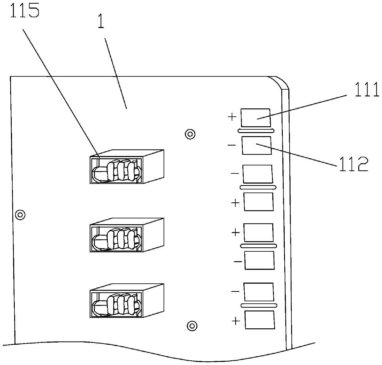
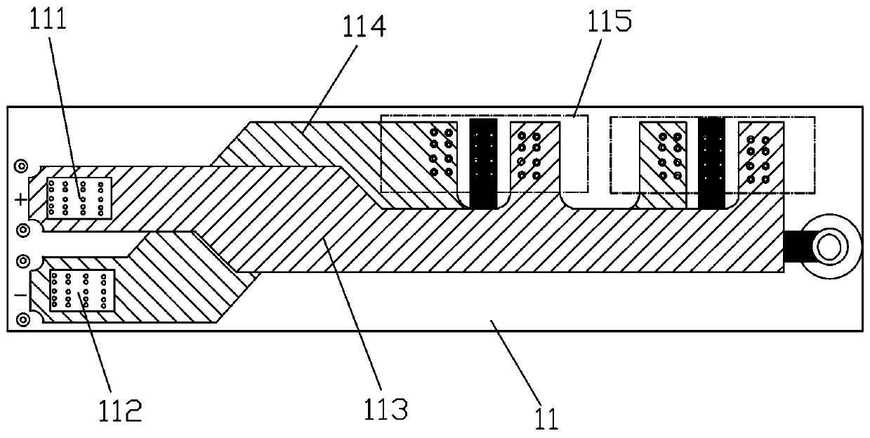
[0034]Such as figure 1 , figure 2 As shown, this embodiment provides a high-power power supply backplane for high-density assembly, including a PCB board 1, and at least one basic power supply unit 11 is formed on the PCB board 1, and the basic power supply unit 11 includes: Welding pad L111, incoming wire pad N112, power supply L layer 113, power supply N layer 114, and at least one power supply interface 115, an insulating medium is filled between the power supply L layer 113 and the power supply N layer 114, and the incoming wire The pad L111 is electrically connected to the power supply L layer 113, the incoming line pad N112 is electrically connected to the power supply N layer 114, and the power supply L layer 113 and the power supply N layer 114 are respectively connected to the power supply interface 115. The L pin and N pin are electrically connected.
[0035] In the above scheme, the incoming line pad L111 and the incoming line pad N112 are used for power supply i...
Embodiment 2
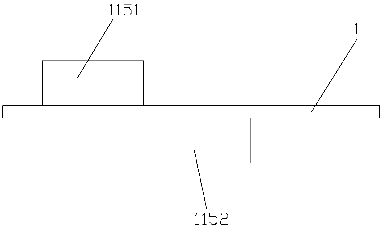
[0039] The difference between this embodiment and the previous embodiment is that, if image 3 , Figure 4 As shown, the basic power supply unit 11 includes a first power supply interface 1151 and a second power supply interface 1152, the second power supply interface 1152 and the first power supply interface 1151 are arranged in a staggered front and back, and are respectively arranged on the PCB board 1 Opposite two sides, and the direction of extension is opposite, specifically as image 3 As shown, the L pin and N pin of the first power supply interface 1151 are electrically connected to the power L layer 113 and the power N layer 114 respectively, and the L pin and N pin of the second power supply interface 1152 are respectively connected to the power supply The power source L layer 113 is electrically connected to the power source N layer 114 .
[0040] Generally, the same basic power supply unit 11 is equipped with two power supply interfaces 115 to meet the high-dens...
Embodiment 3
[0047] The difference between this embodiment and the previous embodiments is that the PCB board 1 includes multiple sets of power layers, wherein one of the power L layers 113 and one of the power N layers 114 form a set of power layers, and each set of power layers The power L layer 113 and the power N layer 114 are arranged axisymmetrically with the central axis of the cross section of the PCB 1, and the two sides of each of the power L layers 113 and the two sides of each of the power N layers 114 Both sides are provided with an insulating medium layer. It is beneficial to change the feeding section of the basic power supply unit 11 by increasing or decreasing the number of power supply layers in groups, wherein the size of the feeding section is determined by the size of the feeding current of the basic power supply unit 11, and the feeding current of the basic power supply unit 11 The size is derived by calculating the power consumption of the plug-in unit. Such as Fi...
PUM
 Abstract
Description
Claims
Application Information


