A high-power power supply backplane for high-density assembly
A high-power, high-density technology, applied in the direction of support structure installation, servers, data centers, etc., can solve the problems of unable to meet the computing load, easy to generate local hot spots, and low PDU power, so as to facilitate mass construction and avoid Local hot spot, good heat dissipation effect
- Summary
- Abstract
- Description
- Claims
- Application Information
AI Technical Summary
Problems solved by technology
Method used
Image
Examples
Embodiment 1
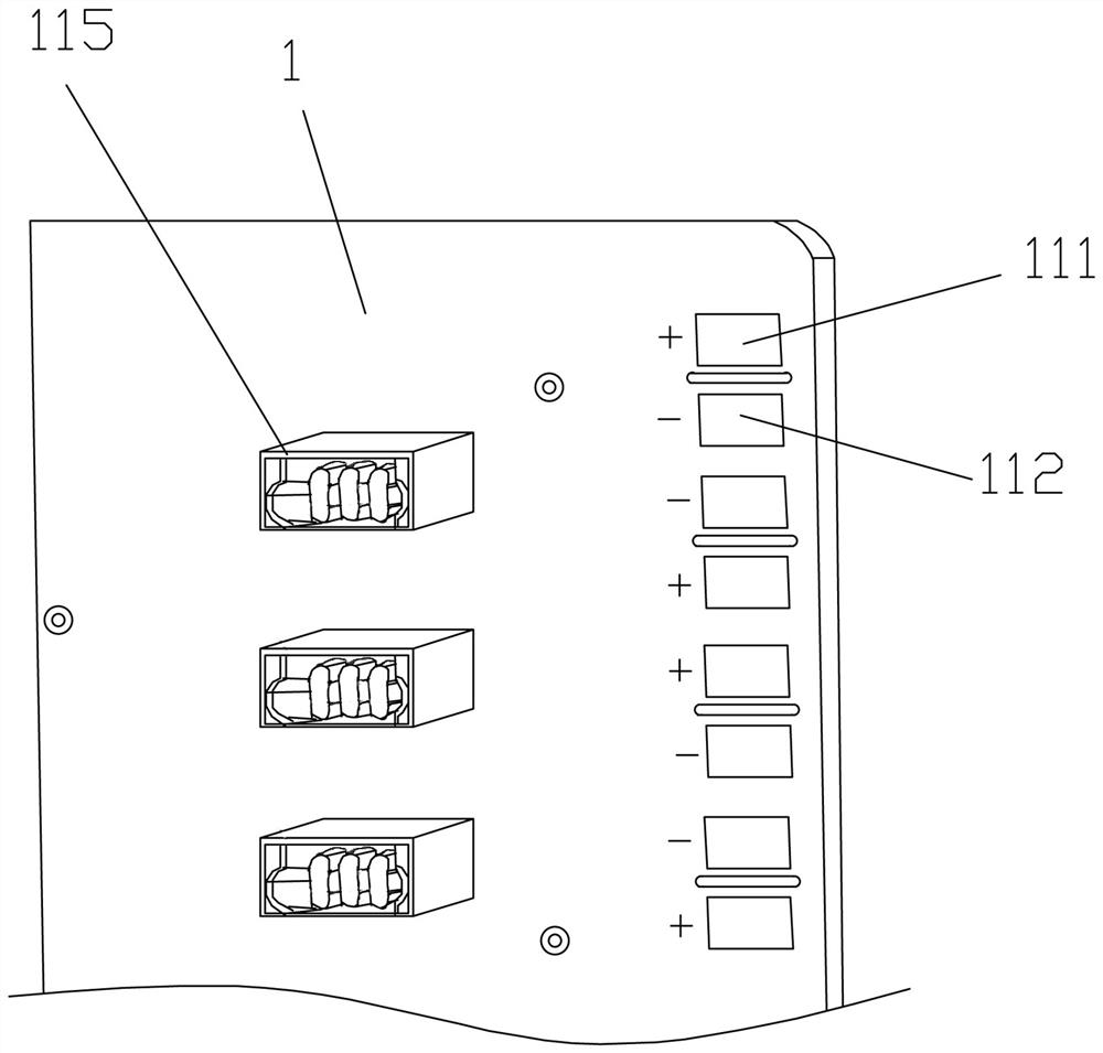
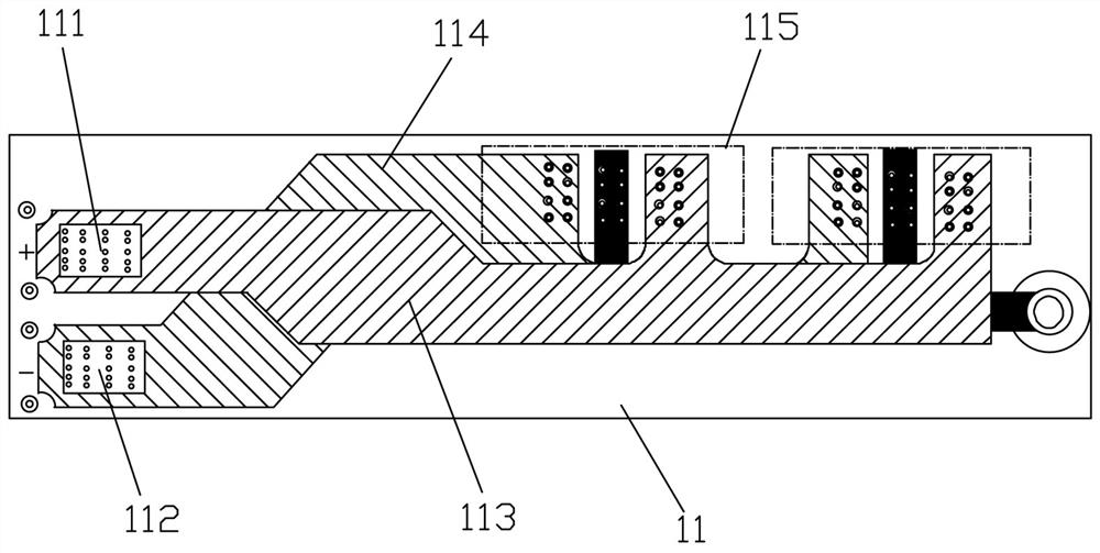
[0034]Such as figure 1 , figure 2 As shown, this embodiment provides a high-power supply back plate facing high-density assembly, including a PCB plate 1, and at least one basic power supply unit 11 is formed on the PCB plate 1, and the basic power supply unit 11 includes: an input line. The pad L111, the injecting pad N112, the power source L layer 113, the power supply N layer 114, and at least one power supply interface 115, the power source L layer 113 is filled with the insulating medium between the power supply N layer 114, the input line The pad L111 is electrically connected to the power source L layer 113, and the input pad N112 is electrically connected to the power supply N layer 114, the power source L layer 113 and the power supply N layer 114, respectively, respectively, respectively, respectively. The l pin and N foot are electrically connected.
[0035] In the above scheme, the adapter pad L111, the input pad N112 supply power supply wire welding, the power supply ...
Embodiment 2
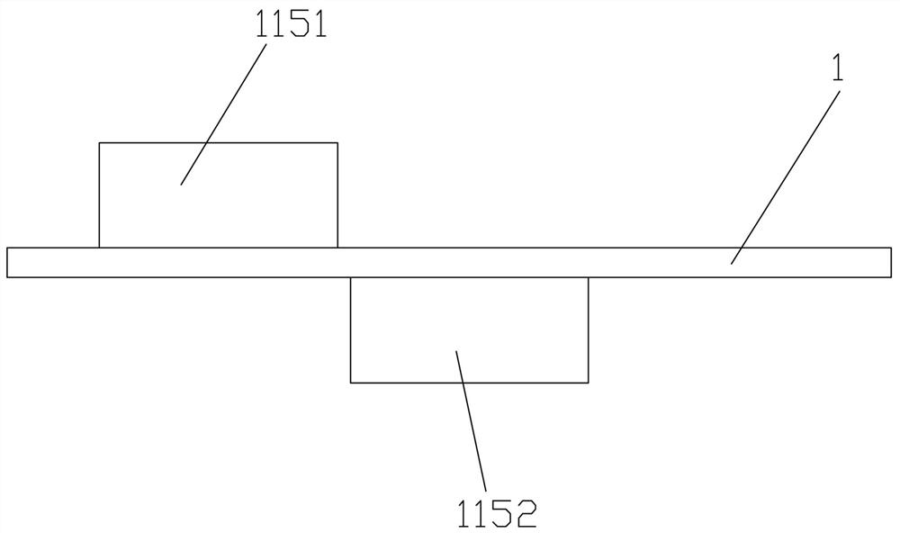
[0039] The difference between the present embodiment and the previous embodiment is, such as image 3 , Figure 4 As shown, the basic power supply unit 11 includes a first power supply interface 1151 and a second power interface 1152, the second power supply interface 1152, with the first power supply interface 1151, with the front and rear displacement arrangement, respectively, respectively, respectively, respectively 1 opposite two sides, and the extension direction is opposite, image 3 As shown, the L-pin and n pins of the first power supply interface 1151 are electrically connected to the power source L layer 113 and the power supply N layer 114, respectively, and the second power supply interface 1152 is respectively The power supply L layer 113 and the power supply N layer 114 are electrically connected.
[0040] In general, the same basic power supply unit 11 is equipped with two power supply interface 115 to satisfy the high-density assembly of the existing cabinet, and the...
Embodiment 3
[0047] The difference from the previous embodiment is that the PCB plate 1 includes a plurality of sets of power supply layers, wherein one of the power supplies L layers 113 and one of the power supply N layers 114 constitute a set of power layers, each set of power layers The power source L layer 113 and the power supply N layer 114 are arranged axis symmetry at the cross-section center axis of the PCB plate 1, both sides of each of the power supplies L layers 113, and each of the power supplies N-layer 114. The insulating dielectric layer is provided on the side. It is advantageous to increase the amount of power layer by grouping to change the feed section of the basic power supply unit 11, wherein the size of the feedth section is determined by the feed current size of the basic power supply unit 11, and the feed current of the basic power supply unit 11 is determined. The size is launched by the power consumption of the calculation plugin unit. Such as Figure 5 As shown, set...
PUM
 Abstract
Description
Claims
Application Information


