Array substrate, manufacturing method and display panel

A technology of an array substrate and a manufacturing method, which are applied in the fields of an array substrate, a manufacturing method and a display panel, can solve the problems of inability to monitor the etching U% of an insulating layer, difficulty in process optimization, increase in cost, etc., so as to improve the process yield and save money. Power consumption, the effect of saving production costs

Active Publication Date: 2020-01-17
KUSN INFOVISION OPTOELECTRONICS
View PDF4 Cites 2 Cited by
  • Summary
  • Abstract
  • Description
  • Claims
  • Application Information

AI Technical Summary

Problems solved by technology

The existing process technology cannot effectively monitor the etching U% of the insulating layer, and it is di

Method used


Image

  • Array substrate, manufacturing method and display panel
  • Array substrate, manufacturing method and display panel
  • Array substrate, manufacturing method and display panel

Examples


Example

[0061] First embodiment

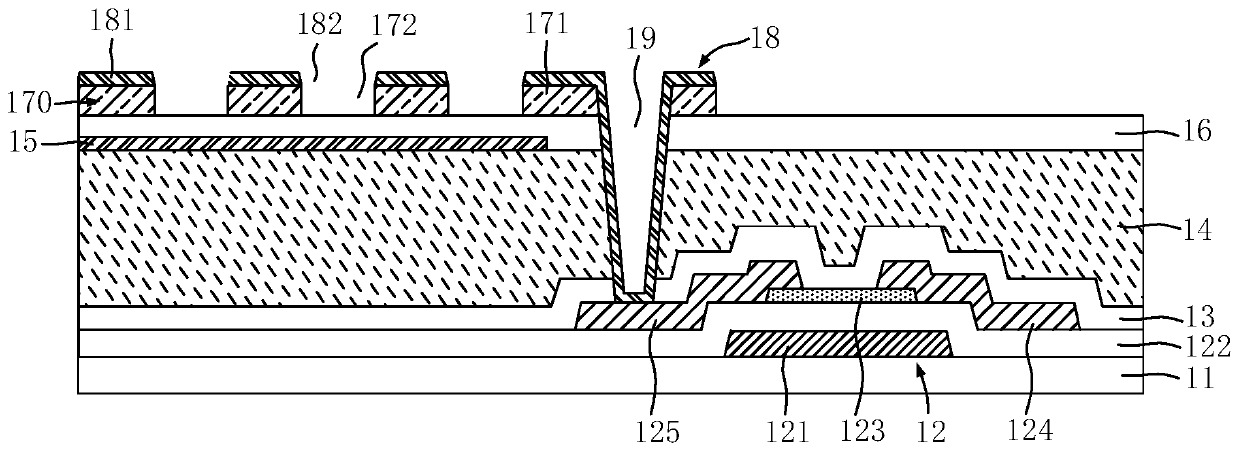
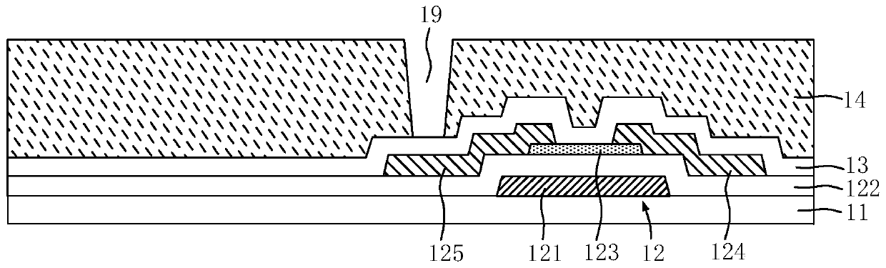
[0062] Figure 2a to Figure 2k It is a schematic diagram of the manufacturing process of the array substrate in the first embodiment of the present invention, which is used to manufacture the above-mentioned array substrate, such as Figure 2a to Figure 2k As shown, the manufacturing method includes: forming a plurality of TFTs 12 arranged in an array on a substrate 11, each TFT 12 includes a gate 121, a gate insulating layer 122, an active layer 123, a source 124 and a drain 125. Specifically, a first metal layer (not shown) is deposited on the substrate 11, and the first metal layer is patterned to form a scan line (not shown) and a gate 121; and the gate is deposited on the substrate 11. The insulating layer 122, the gate insulating layer 122 covers the scan line and the gate 121; an active layer film is deposited on the gate insulating layer 122, and the active layer film is patterned to form the active layer 123, the active layer 123 It can be amorp...

Example

[0069] Second embodiment

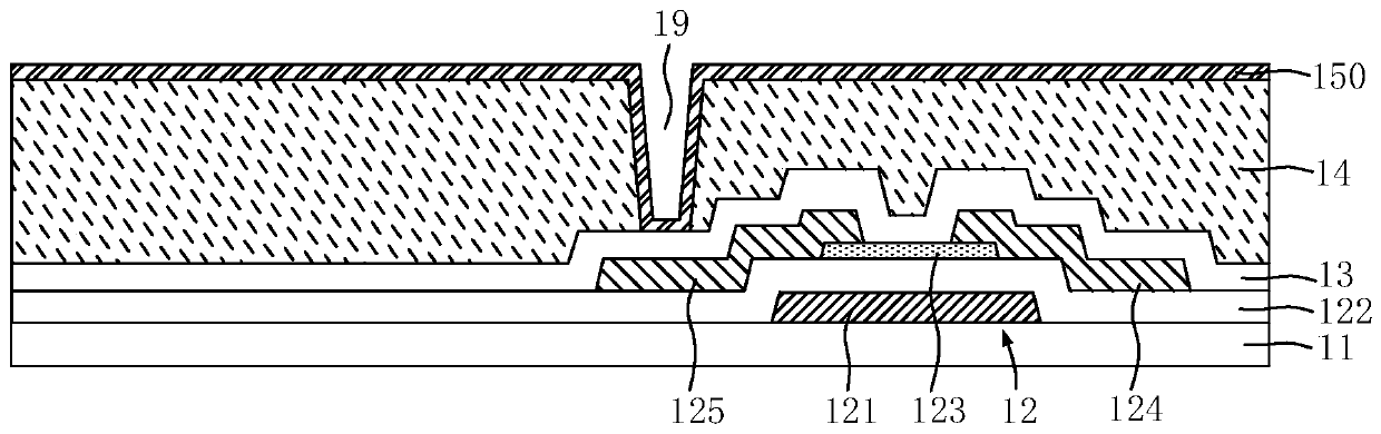
[0070] Figure 3a to Figure 3k It is a schematic diagram of the manufacturing process of the array substrate in the second embodiment of the present invention. The implementation of this embodiment is basically the same as that of the first embodiment, and the similarities are not repeated here. The differences include:

[0071] A second insulating layer 16 covering the common electrode 15 is formed, and the second insulating layer 16 also covers the exposed flat layer 14 and the first insulating layer 13 at the same time;

[0072] A dry etching process is used to remove the second insulating layer 16 at the position of each contact hole 19 to expose the first insulating layer 13 below at the position of each contact hole 19;

[0073] A third insulating layer 17 covering the second insulating layer 16 is formed. The third insulating layer 17 also covers the exposed first insulating layer 13. The second insulating layer 16 is made of a material that can be dr...


PUM


Abstract

The invention provides an array substrate. The array substrate is characterized in that a common electrode of the array substrate is covered with a second insulating layer; a third insulating layer isformed on the second insulating layer; multiple pixel electrodes are formed on the third insulating layer at intervals, and each pixel electrode is conductively connected with one corresponding TFT through a contact hole; wherein each pixel electrode is of a patterned structure with a pixel electrode strip and a first slit; the third insulating layer is etched to form a plurality of insulating layer patterns at intervals, each insulating layer pattern corresponds to one pixel electrode strip, the insulating layer patterns and the pixel electrode strips have the same pattern and are mutually overlapped up and down, the second insulating layer is made of a material capable of being subjected to dry etching, and the third insulating layer is made of a material capable of being subjected to wet etching. The invention further provides a manufacturing method of the array substrate and the display panel. According to the array substrate, the problem of film thickness uniformity after the insulating layer is etched can be solved, so that the difference of driving voltages in different areas in a plane is reduced.

Description

technical field [0001] The invention relates to the field of display technology, in particular to an array substrate, a manufacturing method and a display panel. Background technique [0002] Liquid crystal display (liquid crystal display, LCD) has the advantages of good picture quality, small size, light weight, low driving voltage, low power consumption, no radiation and relatively low manufacturing cost. Almost all kinds of portable electronic products use LCD as Display panels, which dominate the field of flat panel displays. [0003] Existing display panels usually include a color filter (CF, Color Filter) substrate, a thin film transistor (TFT, Thin Film Transistor) substrate, and a liquid crystal (LC, Liquid Crystal) sandwiched between the color filter substrate and the thin film transistor substrate. [0004] Thin film transistor liquid crystal displays (TFT-LCDs) can be classified into a vertical electric field type and a horizontal electric field type according to...

Claims


Application Information

Patent Timeline
IPC IPC(8): H01L21/84H01L27/12G02F1/1362
CPCH01L27/1259H01L27/1248H01L27/1244H01L27/1288G02F1/136227
Inventor 钟德镇郑会龙张军杨国栋
Owner KUSN INFOVISION OPTOELECTRONICS
Why Eureka
Try Eureka