CMOS-TDI image sensor and forming method thereof

An image sensor and substrate technology, applied in the direction of electric solid-state devices, semiconductor devices, electrical components, etc., can solve the problems of voltage domain noise improvement and poor performance, and achieve the effects of reducing dark current, improving efficiency, and improving image quality

Inactive Publication Date: 2020-01-24
BRIGATES MICROELECTRONICS KUNSHAN
View PDF4 Cites 0 Cited by
  • Summary
  • Abstract
  • Description
  • Claims
  • Application Information

AI Technical Summary

Problems solved by technology

The output voltage signals of all M rows are accumulated. For an M-class TDI image sensor, the signal is increased by M times, but the noise in the voltage domain is also increased.
[0005] However, the performance of existing CMOS-TDI image sensors is still poor

Method used


Image

  • CMOS-TDI image sensor and forming method thereof
  • CMOS-TDI image sensor and forming method thereof
  • CMOS-TDI image sensor and forming method thereof

Examples


Embodiment Construction

[0029] As mentioned in the background art, the performance of existing CMOS-TDI image sensors is still poor.

[0030] The following will describe in detail in conjunction with the accompanying drawings.

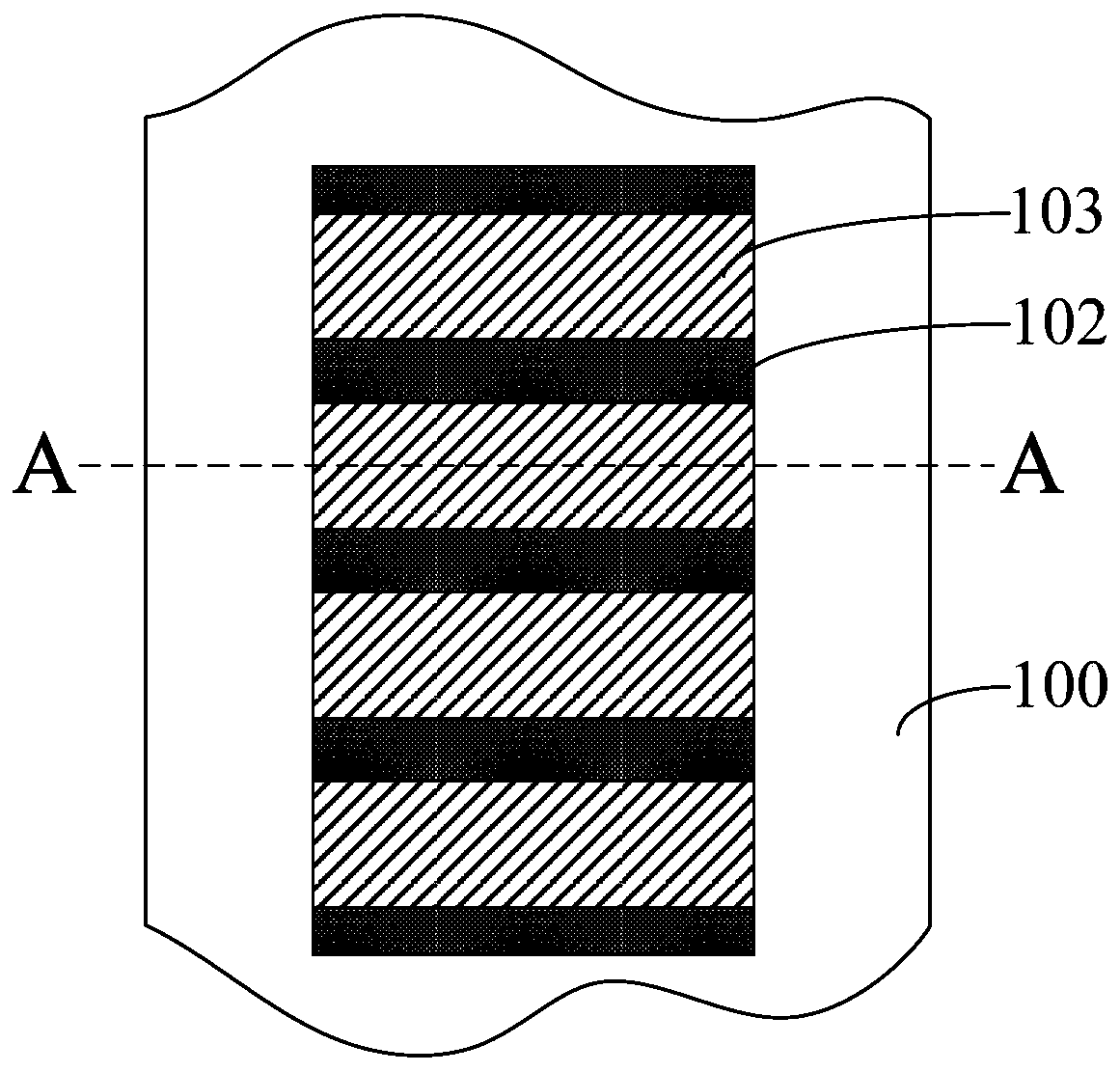
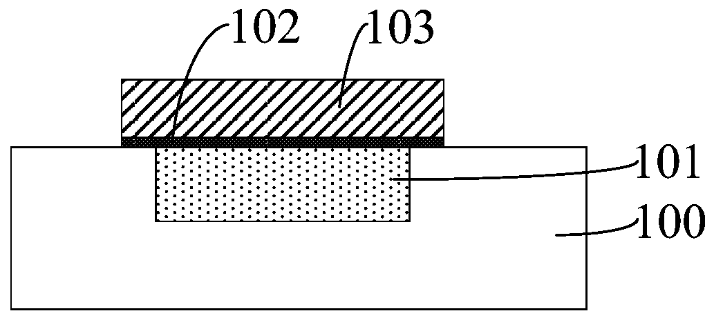
[0031] Please refer to figure 1 with figure 2 , figure 2 yes figure 1 A schematic cross-sectional structure along the A-A line, providing a substrate 100; forming a photoelectric doped region 101 in the substrate 100; forming a gate structure on the surface of the photoelectric doped region 101, the gate structure includes a gate dielectric layer 102 and The gate layer 103 located on the gate dielectric layer 102 .

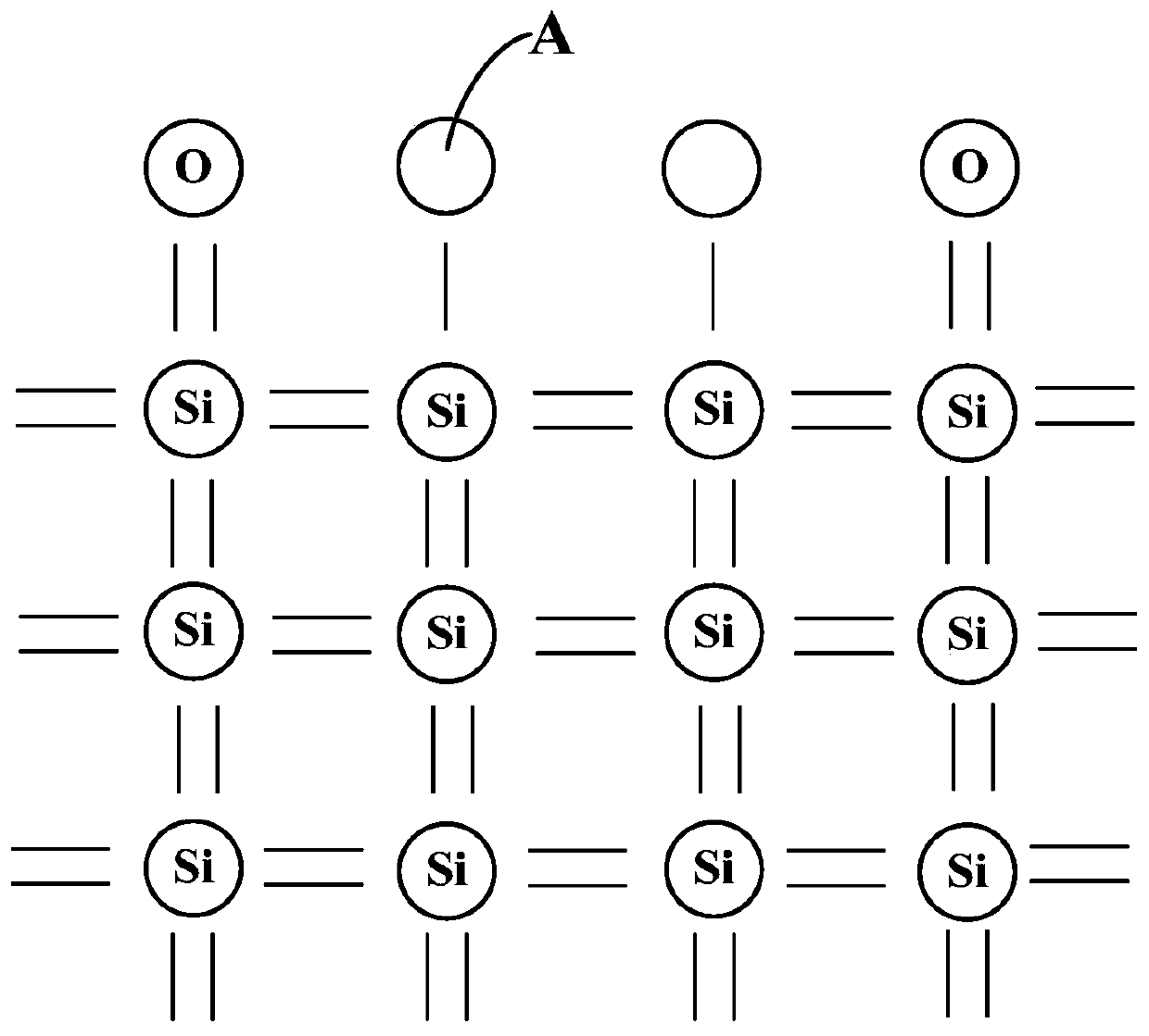
[0032] Please refer to image 3 , in the above embodiment, the material of the substrate 100 is silicon (Si), and the material of the gate dielectric layer 102 is silicon oxide (SiO 2 ), in the CMOS-TDI image sensor, due to the special requirements on the manufacturing process, the passivation layer cannot be formed on the surface of the substrate 100, so...


PUM

PropertyMeasurementUnit
thicknessaaaaaaaaaa
thicknessaaaaaaaaaa

Abstract

The invention provides a CMOS-TDI image sensor and a forming method thereof. The forming method comprises the steps: providing a substrate; forming a photoelectric doped region in the substrate; forming a plurality of gate structures on the surface of the photoelectric doped region, wherein each gate structure includes a gate dielectric layer and a gate layer located on the gate dielectric layer;and performing the doping process at the interface between the gate dielectric layer and the substrate, wherein the doping process is used for reducing the defects between the gate dielectric layer and the substrate. According to the technical scheme, the doping process is performed at the interface between the gate dielectric layer and the substrate so that the defects formed by the substrate andthe gate dielectric layer are combined with the second ions in the doping process to realize play the passivation effect and thus the generation of dark current can be reduced and the image quality of the CMOS-TDI image sensor can be improved.

Description

technical field [0001] The invention relates to the technical field of semiconductor manufacturing, in particular to a CMOS-TDI image sensor and a forming method thereof. Background technique [0002] A Time Delay Integration (TDI) image sensor is an evolution of a linear image sensor. The imaging mechanism of the time-delay integral image sensor is to expose the pixels passed by the object one by one, and accumulate the exposure structure, so as to solve the problem of weak imaging signal caused by insufficient exposure time of high-speed moving objects. The time-delay integral image sensor can increase the effective exposure time and improve the image signal-to-noise ratio. [0003] There are two types of time-delay integral image sensors, CCD and CMOS. However, due to the particularity of the CCD process, other processing circuits cannot be integrated on the image sensor, and the versatility and flexibility are poor. [0004] Another type of TDI image sensor is a CMOS ...

Claims


Application Information

Patent Timeline
Patent Type & Authority Applications(China)
IPC IPC(8): H01L27/146
CPCH01L27/14605H01L27/14643H01L27/14689
Inventor 黄金德王林胡万景
Owner BRIGATES MICROELECTRONICS KUNSHAN
Why Eureka
Try Eureka